Organic Heterojunctions in Solar Cells
| Previous Topic | Return to OPV Menu | Next Topic |
A heterojunction is the contact of two materials with different electrical properties. These materials could be polymers or small molecules and both types are used in our research. The donor is more electron rich than the acceptor. When the donor is excited by light it causes a negative charge in the acceptor while the donor becomes positively charged. The positive charges move by hole hopping, and the negative charges by electron hopping via charge transfer between molecules. Thus charges move in the organic layers which force charge to move in the electrodes.
Materials used in Organic Heterojunctions
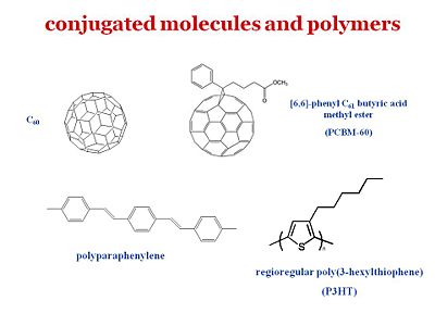
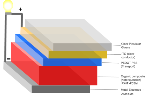
For organic solar cells and organics light emitting diodes, the materials belong to the same two types of schools. One type uses small molecules that you can vapor deposit in a vacuum. Another consists of uses polymers can be processed through wet chemistry. A ubiquitous component as an electron acceptor is Fullerene or C60. In particular, this derivative of C60 provides for a much better compatibility with the other components. Therefore c60 is an excellent electron acceptor and what is left needed is an electron donor. It is found that if you just use C60 it will usually face segregate. Where as if C60 or C70 is prepared as a PCBM there that provides for a much better compatibility and the ability to have better quality blends with a donor polymer such as polyphenyl vinylene (PPV) or a polythiophene such as the regioregular poly(3-hexylthiophene) (P3HT)
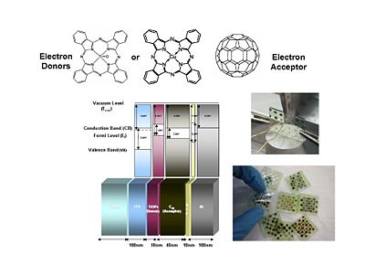
So PPV and P3HT in the polymer form or in the oligomer form are frequently used as electron donors. C60 is the electron acceptor but there are other systems. For instance Bernard Kippelin and his group have been able to design and fabricate excellent solar cells based on C60 as the acceptor and pentacene as the donor.
See review article Gunes 2007 [1]
Energy levels in heterojunctions
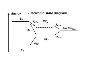
The literature refers to the exciton states and the charge transfer state which is when the donor + and the acceptor – are right next to each other. But the electron and the hole still feel each other rather strongly. This charge transfer state CT1 is the lowest in energy precisely because the electron and the hole are strongly bound together. Remember, the stronger the attraction between the + and – charges, the lower the energy state. So the lowest energy charge transfer state has the strongest coulomb attraction between the hole and electron. To separate the charges, energy must be applied and a higher energy state must be acquired. In the literature there are many models that demonstrate how this can be achieved. But it would be much simpler to go directly from S1 to higher lying charge states CTn and then to CS=Efinal rather then going all the way down to CT1 and then to the final state.
With atomic energy levels, the higher the energy level of a state, the farther away the electron is from the nucleus. Compare this with CT: the higher the energy of a charge transfer state, the lesser the attraction is between the electron and the hole, and the further away the two species are from one another. So if a higher lying charge transfer state is achieved, that state will be more diffused and the wave functions will be more delocalized. Alternatively, if instead of the exciton occurring at the interface and the charges being right next to each other, if the plus is further from the minus because the wave functions are more delocalized, it will be easier for the plus and minus to move away from one another.
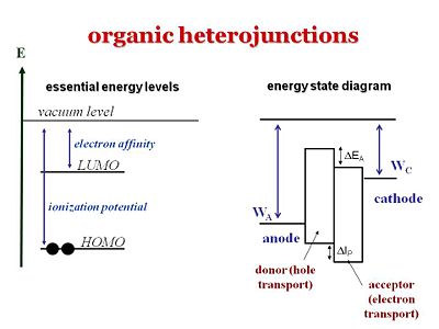
It is important to understand the differences between the levels that refer to one electron level picture and states that refer to the whole molecule or system. The ionization potential of a molecule can be approximated as the HOMO, the energy or the inverse of the energy of the HOMO level. The electron affinity can be related to the energy of the LUMO level. But one must not forget that the ionization potential and electron affinity are characteristics of the whole molecule.
Homo and Lumo
The energy state diagram refer to states, the difference in energy between the ground state and the ionized state of the whole molecule. Where as HOMOS and LUMOS refer to electron levels. When organic solar cells are discussed, we must pay attention to the electron affinities and ionization potentials of the donor and acceptor components. The ionization potential of the donor is the difference between the neutral molecule and the energy it takes to take away an electron from that molecule. HOMO and LUMO levels are often seen in the literature but these are only approximations. We need to take into account are the ionization potentials and the electron affinities of both the donor and the acceptor. In order for this concept of the donor and acceptor to be valid, the ionization potential of the donor should be lower than that of the acceptor because the donor is the species that most easily gives away an electron. In this diagram the ionization energy of the donor is the distance between to top of the donor band and the vacuum level band above. Conversely, the electron affinity of the acceptor should be larger than the electron affinity of the donor.
The photovoltage (Voc) is dictated by the relative HOMO (ionization potential) energy level of the donor and the LUMO (electron affinity) of the acceptor.
<math>V_{oc}= (\frac {1}{ e})(|E^{Donor}HOMO |-|E^{PCBM}LUMO|)-).3V\,\!</math>
Voltages with OPVs are typically very low so many layers in series may be required. Heeger group recently developed a repeated multilayer that effectively double the voltage and allowed for a second donor pigment that could harvest a different part of the spectrum.
See Heeger 2007 [2]
Selecting Donor and Acceptor energy levels
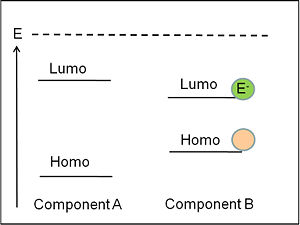
A favored situation is shown where the LUMO of the donor is higher than the LUMO of the acceptor, and the HOMO of the donor is higher than that of the homo of the acceptor. This is a situation where charge separation might be possible but it doesn’t guarantee that it will happen. It is a necessary but it not sufficient condition. For charge separation to occur the combination of these differences in electron affinities and ionization potentials must have the ability to overcome the exciton binding energy. For example in the case of ppv and cyano ppv the levels that are aligned like this but still there is no charge separation. There is energy transfer but no charge separation.
Consider these structures in the absence of any external field. There are two semi conductors, with a work function of the anode, and the work function of the cathode. The work function refers to the Fermi level that is the chemical potential of the two electrodes. When a system is in equilibrium, the system tends to get the chemical potentials to be the same across the entire system. In order to reach an equilibrium, the system will tend to have some charge redistribution that will increase chemical potential on the anode side and decrease the potential energy on the cathode side so that the two chemical potentials can try to align.
Since the chemical potential of the anode and the cathode are different, there will be some charge redistribution to increase the energy on the anode side and decrease the chemical potential on the cathode side. This will create a bias of the levels within the organic semiconductor or insulators, which is called a built in potential or built in electrical field. In the physics literature, a description of what is happening can be found in the context of metal insulators and metal structures. If there is an elimination and an electron hole pair is formed at the interface, the electron will travel to the acceptor side, and a hole will be left on the donor side. This built-in potential makes the electron drift towards the cathode and the hole drift towards the anode. Without that built-in field, there will be no incentive for the electron to drift one way or the other; the electron and hole would diffuse. However, the built in potential gives a direction for the motion of the separated charge carriers.
Geometries of excitonic solar cells
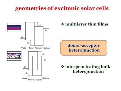
Recently, there were steady improvements in efficiencies of organic solar cells. Whether it is based on multilayer thin film geometry or intepenerating polymer blend, the efficient light harvesting relies on donor-acceptor heterojunction in most cases. Therefore, it is our purpose to establish the model that characterizes the photoelectrical response of the cellls based on those donor-acceptor heterojunctions.
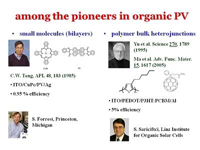
These are the two major geometries that have been considered. For example, from Chin Tang’s paper in 1986, one of the geometries included a bi-layer: it had an anode, cathode, donor component, and an acceptor component. The idea of Chin Tang is to move away from a homojunction that uses a single component, and go to a two component system with a donor and an acceptor. However, an issue with this type of system is that the diffusion length must be quite large in order for the exciton to reach the interface and disassociate. It is possible to make the layer thinner so that the distance to the interface is shorter, but in doing so, the layer will be less absorbing and fewer photons will be absorbed.
A typical multilayer device is built on glass or plastic substrate. First a layer of transparent, conductive indium tin oxide (ITO) as an electrode, A thalociline donor molecule, and then an acceptor layer containing buckyballs and lastly an opaque aluminum electrode. Light shines through the glass and the ITO, is absorbed by the donor, charge is passed to the acceptorand then finally to the aluminum electrode.
See review by Forrest [3]
Bulk heterojunctions
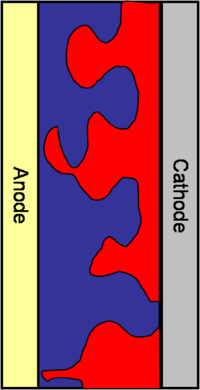
So the idea in the mid 90’s, from the group of Allen Heegger in Santa Barbara, was to build a bulk heterojunction. Bulk heterojunctions are made by creating interpenetrating networks of the donor and the acceptor components. With the two components interpenetrating one another, an exciton will never be far from the interface. In addition, with respect to the volume, the surface represented by the interface will be larger. The interfacial area will be large and the diffusion length of the excitons can be short. This puts many constraints on how to manage the morphology of the interpenetrating network. This is due to the fact that once the disassociation has taken place, the electron and the hole need to have a clear path to get to the cathode and the anode respectively. If the morphology is such that the path closes somewhere along the way, the electron and the hole will be lost. Bulk heterojunctions, are described as systems of interpenetrating “fingers” of the donor component and the acceptor component sandwiched between the anode and cathode. This system has a large interfacial area, the interface is not far from where the exciton is generated, and once the exciton disassociates, the electron and the hole will have a clear path to their respective electrodes. Creating perfecting aligned interdigitating fingers is a challenge for material designers. In practice the interface is much more uneven and the path the exciton must take is perilously long.
You are often are limited by the diffusion length of the exciton. All these factors contribute to why people have spent so much time trying to design efficient bulk heterojunctions. The morphology must be controlled so that the electron and the hole can always go back to the cathode and anode respectively. Also there should not be many places where the hole and the electron see each other and can recombine.
Another problem is that of phase separation of the heterojunction blend, which decreases performance.
Pioneers in organic photovoltaics
There are a few people who have advanced the field. Chin Tang used to work for the Kodak research center but moved to become a full professor at University of Rochester in 1986. There have also been major advances from Steve Forrest who was at Princeton for quite some time and had recently transferred to his alma meter as VP for research at Michigan. In terms of polymers, a major step forward in understanding was made when Serdar Sariciftci was working as a research scientist in Allen Heeger’s groups in the early 90’s. They discovered an ultra-fast charge separation at the interface between a PPV derivative and C60. The charge separation occurred within about 30 – 40 femptoseconds. Since the charge separation is so much faster than any other process, it leads to a charge separation of unity. That is why there has been so much work on phenyline, vinylines with c60 or c60 derivatives as well as more recently on polythiophenes or derivatives thereof and C60 and derivates thereof.
References
| Previous Topic | Return to OPV Menu | Next Topic |
