Major Processes in Organic Solar Cells
| Previous Topic | Return to OPV Menu | Next Topic |
Edmond Becquerel (1820-1891) was first to discover the photovoltaic effect. But it took quite a long time before there was a report on an efficient cell and that came from Chapin, Fuller and Pearson (1954) in Bell Labs. They reported a silicon cell with 6% efficiency.
Semiconductors compared
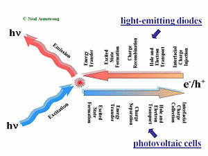
This slide gives a comparison of the processes that are placed in LED in a solar cell and in a field-effect transistor. The first step of the process required charge injections in the electrodes, holes injected from the anode, and electrons injected from the cathode. Those holes and electrons then migrate to diffuse in the presence of an external electric field due to the applied voltage across the organic layer or layers. Then the hole and the electron have to find one another to recombine. That leads to the formation of an excited site, an exciton. During its lifetime, the exciton can also hop from chain segment to chain segment or molecule to molecule. This is called an energy transfer. If all goes well, a decay to the ground state will occur radiatively and a photon will be released. This step is necessary; photons that are produced within the device must be released to see any visual information.
A photovoltaic cell works in reverse to a light-emitting diode. While in a light emitting diode an electrical current is injected into the material and transformed into photons, a photovoltaic cell requires an absorption of the photons to generate an electrical current. The photovoltaic cell first absorbs photons, which leads to a formation of excitons in an excited state. These excitons move to the interface between the donor component and the accepter component in the organic solar cell. At the interface of the donor and accepter, the exciton disassociates so that the hole and the electron become free from one another. The separated hole and electron will be diffused within the material and get collected by the electrodes.
The major processes occur in reverse order but there is one major difference; any organic material, or combination of materials that’s good for luminescence and thus good for light emitting diode will be bad for organic photovoltaic cells. The reason is that in a light-emitting diode, an electron and the hole approaching each other is favorable. This will form the exciton that will decay and lead to photon emission. On the other hand in the case of a photovoltaic cell, separation of the electron and hole is favorable so they can migrate to the opposing electrodes. These two steps are entirely different in the two types of systems.
Field effect transistors
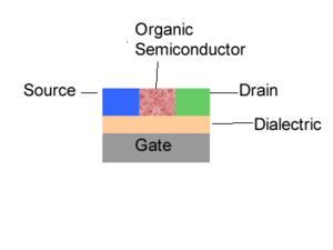
When you look at the field-effect transistors there are three major processes. The first one is the injection of charges into your semi-conductor. In the case of light-emitting diode and photovoltaic cell there are only two electrodes. However, in a field-effect transistor, the charge injection is modulated through a third electrode called a gate. Now all is needed are the electrons and the holes. Let’s suppose you inject electrons. Those electrons must migrate and be collected. The first electrode will be referred to as a gate. Then you have a thin insulator called a dielectric. You have two other electrodes referred to as the source and the drain. Then you have your organic semi-conductor. This is one of the configurations possible. When you are given a voltage difference between the source and drain, the amount of charges that will be injected into your semi-conductor will be modulated by the voltage at the gate. The gate will modulate the injection and produce a switching effect. For a given voltage between the source and drain, the voltage of the gate can either be decreased such that there is a small injection or current or it can be increased to have a very large injection of charges into your semi-conductor and a large current. These are the components that make a transistor, which is also called a three terminal devices because you have 3 electrodes. So once you have an injection of charges into the organic semi-conductor, those charges will travel and be collected at the other electrodes. These are the main steps in an organic semi-conductor; charge injection, charge transport, and charge collection.
Quantifying OPVs
Exciton binding energies
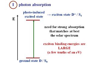
It is important for the material to absorb photons efficiently in the energy region that matches at best the solar spectrum. If you look at the solar spectrum, it goes very significantly into the Near IR. That means a pretty small bandgap system that can get down to 1 EV bandgap absorbing nearly down to 1 electron-volt. If you have a material that has a bandgap in the middle of the visible, then you will miss out on a lot of photons.
Also, the photon density shows that there are few photons that can be absorbed with energies like 4 electron volts. If the energy is very large, there are fewer photons. This requires a good match between the solar spectrum and the longer wavelengths with lower energies. In the case of π-conjugated systems the exciton binding energies are large about a few tenths of an eV. This is what makes the difference with the respect to the organic semi-conductor. The exciton binding energy in silicon or gallium arsenide is just a few milli -eV. Thus at room temperature, there is enough energy to allow the electron and the hole to separate.
Photovoltaic Efficiency
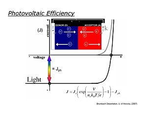
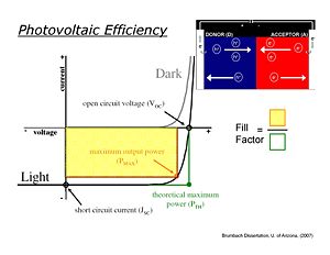
Photovoltaics efficiency can be described using a current voltage curve-- the voltage on the x axis and the current on the y axis. In the dark the device has very little current flowing (gray line). The forward bias region is to the right of the axis. When voltage is increased at past a critical onset voltage certain point the current begins to rise exponentially. This is the same with any diode build with build with two dissimilar electronic materials. When light is turned on the curve shifts down (black line) producing a photocurrent identified as Jph. The intersection with the Y axis is the short circuit photocurrent. The intersection with the x axis is the open circuit voltage which is the largest voltage the cell can generate. The behavior is governed by the Shockley equation. The dark current/voltage curve is simply displaced by an amount when light is applied.
Photovoltaic maximum power
Power is the product of voltage of current. If this were an ideal cell the maximum power would be the product of the open circuit volage and the short circuit current (PTH). We actually get a maximum power point on the curve. The fill factor is ratio of the maximum output measured vs the theoretical maximum. A fill factor of .7 or .8 is as good as you get with any solar cell. OPV have fill factors around .5 or at the most .6. The fill factor is determined by the shape of the curve, which is in turn governed by how fast the charges recombine before we can harvest the current.
Steps of Organic Photoelectric Process
Light absorption (exciton formation)
Suppose you have a crystalline silicon that absorbs a photon from the solar spectrum, which leads to an excited state. The exciton binding energy is so small that the electron and hole can separate and thus, a current can be produced. However, in an organic material, the absorption of a photon creates a strongly bound exciton. Remember that an exciton is a neutral species. When you have the electron and the hole next to one another, the charge is 0 since 1+ + 1- = 0. A current can not be generated from an exciton. This is why crystalline silicon can perfectly lead to an absorption to the generation of free carriers also known as band to band process. Suppose you form an exciton on a polythiophene chain. To generate a current, you must disassociate the exciton, meaning, separate the electron and the hole in the exciton so that they can move away from one another and generate current.
Exciton Migration
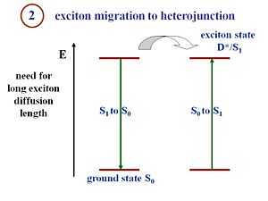
This is the key point that makes the processes in an organic solar cell different from the processes in a crystalline silicon or amorphous silicon solar cell. That is the fact that in the pi- conjugated materials, you have large binding energies. Excitons must be formed and disassociated to generate a current. The structure of the organic cells includes a component that corresponds to an electron donor and a component that corresponds to an electron acceptor. There is an interface between those two components where the excitons must reach in order to disassociate. The critical condition for an efficient organic solar cell is the fact that the exciton can diffuse a pretty large distance within its lifetime. If the interface on average is 20 nanometers from where the exciton is generated, but during its lifetime the exciton only diffuses 5 nanometers, no current will be produced. You will have photons in and photons out or vibrations out or anything similar but a current will not be generated. In other words, during its lifetime, the exciton must be able to diffuse and reach the interface between the donor and acceptor components. If a system is designed with large diffusion lengths and the migration of the exciton takes too long, then the average distance between where the exciton is generated and the interface can be reduced. This results in thinner films. However, if the film too thin, only a few number of photons can be absorbed. This is a type of issue many organic cells engineers deal with. The film must be thick enough to absorb a reasonable amount of photons, but simultaneously, the film must also be thin enough so that the generated excitons can reach the interface efficiently.
Charge separation (exciton dissociation)
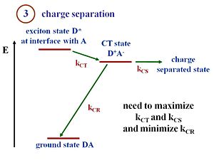
This state diagram shows what happens when the exciton reaches the interface. The D refers to the donor component and A refers to the acceptor component. At the interface there are donor molecules or donor polymer chains next to the acceptor molecules or acceptor polymer chains. The lowest energy state is the ground state of the two components. Suppose that the exciton is formed within the donor. This exciton will be labeled D*, an excited state in the donor. The exciton must reach the interface. There is a state and energy there that corresponds to the exciton energy above the ground state. What needs to happen is that the exciton at the interface must get into a charge transfer state in which then the electron finds itself on the electron acceptor and therefore, there is a hole on the donor component. Now we have what we call a charge transfer state D+ A-. The + and – now need to move away from one another. This process is called a charge separated state. So you need not only to have a charge transfer but to have a charge separation. In the literature, the use of these terminologies can be confusing depending on the community you from a state like this could be in a molecule. For instance, people might say this is a charge separated state. It is possible to have a charge transfer state where the + and the – remain close to each other. However, in order to generate a electrical current a full separation of the + and the – is needed. So that is the distinction between a CT(Charge transfer) state and a CS(Charge separation) state shown on the diagram/slide. At the CT state, when the hole and electron, the D+ and A-, are next to each other, there is a chance that they will recombine (aka recombination) and lead to the ground state. If this happens a loss in terms of efficiency of the charge separation process will occur. Recombination is the main reason for the low efficiencies of OPVs.
The goal is to maximize kct(charge transfer) and kcs(charge separation) and minimize kcr(charge recombination). The rate of transfer and of charge separation need to be maximized while the rate of charge recombination must be minimized. With those rates, you can also evaluate the Marcus Theory expressions.
Charge Migration
Inorganic solar cells can be very efficient because a single inorganic material can be used with an exciton binding energy is negligible at room temperature. The physics of organic solar cells very different because the exciton is strongly bound. You need to have an acceptor and donor component with as much interface as possible between them in order that the formed excitons can quickly reach the interface to disassociate.
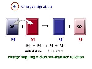
Once the excitons have disassociated into two separated species, the electron and the hole, they must move efficiently toward the electrodes. Remember that the more you can order your material, in general, the better the mobility will be. The faster the electrons and the holes can move away from each other, the more efficient their separation will be.
Electronic energy Levels
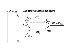
In the literature, people will refer to the exciton states and the charge transfer state which is when the donor + and the acceptor – are right next to each other. But the electron and the hole still feel each other rather strongly. This charge transfer state CT1 is the lowest in energy precisely because the electron and the hole are strongly bound together. Remember, the stronger the attraction between the + and – charges, the lower the energy state. So the lowest energy charge transfer state has the strongest coulomb attraction between the hole and electron. Therefore, to separate the charges, energy must be applied and a higher energy state must be acquired. In the literature there are a number of models that can show how this can be achieved. But it would be much simpler to just go from S1 to higher lying charge states CTn and then to CS=Efinal rather then going all the way down to CT1 and then to the final state. With atomic energy levels, the higher the energy level of a state, the farther away the electron is from the nucleus. By making the connection and comparing with the atomic energy levels, the higher the energy of a charge transfer state, the lesser the attraction is between the electron and the hole, and therefore, the further away the two species are from one another. So if a higher lying charge transfer state is achieved, that state will be more diffused; the wave functions will be more delocalized. If instead of having the exciton come at the interface and then having the plus and minus right next to each other instead the plus is far removed from the minus because the wave functions are much more delocalized, you can intuitively understand that it will be easier for the plus and minus to move away from one another. So this is the picture that is now discussed in the literature.
| Previous Topic | Return to OPV Menu | Next Topic |
