Difference between revisions of "Organic/Organic Heterojunctions in OLEDs"
Cmditradmin (talk | contribs) (New page: This simplistic energy diagram shows what happens to an organic film that is sandwiched between two contacting electrodes. One side is indium tin oxide and the other is aluminum. We are ma...) |
|||
| (24 intermediate revisions by 4 users not shown) | |||
| Line 1: | Line 1: | ||
<table id="toc" style="width: 100%"> | |||
<tr> | |||
<td style="text-align: left; width: 33%">[[The First OLEDs|Previous Topic]]</td> | |||
<td style="text-align: center; width: 33%">[[Main_Page#Organic_Light_Emitting_Diodes|Return to OLED Menu]]</td> | |||
<td style="text-align: right; width: 33%">[[OLED Charge Mobilities|Next Topic]]</td> | |||
</tr> | |||
</table> | |||
==Single-Layer OLEDs Band-Edge Offsets vs. Contact Electrodes== | |||
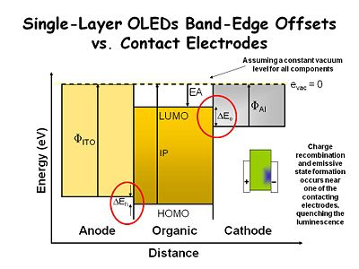
This simplistic energy diagram describes an organic film sandwiched between two contacting electrodes. The anode is indium tin oxide ([[indium tin oxide|ITO]]) and the cathode is aluminum. We assume there is constant vacuum level for all components, although this is not precisely correct. The ITO has a work function represented by the vertical arrow. For clean ITO this is typically 4.7 - 4.8ev. For dirty ITO it can be a low as 4- 4.2ev. The work function for Al is about 4.1ev. The work function difference between the layers allows the aluminum to inject electrons into the organic layer, while the ITO layer injects holes into the organic layer. The work function offset also helps dictate the voltage needed to activate the device. | |||
[[Image:OLED5-singlelayer.jpg |thumb | 400px|Band Edge Offsets]] | |||
The energy offset (ΔE<sub>h</sub>) is the organic layer's ionization potential, defined as the energy required to take an electron out to vacuum. This can be measured with a UV photoelectron spectrometer. There is typically not a good energy match between the ITO bottom contact and the organic layer, causing a small energy barrier that must be overcome in order to inject holes into the organic layer. | |||
The organic layer's electron affinity (EA) is the distance between the vacuum level and the LUMO state, defined as the energy needed to acquire an electron. Cathode materials have a bigger offset (ΔE<sub>e</sub>) between the work function of the electrode and the electron affinity level. This is the energy barrier for injecting electrons into the organic layer. The same phenomenon occurs in an electrochemical system with a concentrated electrolyte solution, but it can be overcome by setting up an electrical double layer at the interface. The steep potential gradient at the interface makes it possible to get an electron injection regardless of the electrode work function. However in condensed phase environments, which have very low dielectric constants and no added ionic species, these energy levels are significant. Tunneling charges through the energy barriers, or thermionic emission becomes necessary to lower drive voltages. | |||
In early experiments with single crystal anthracene, the charge from the anode and the charge from the cathode did not move at the same rate. In this example, the positive charge electrode which injects holes created a charge carrier that moves faster than the electron carrier. As a result most of the recombination occurs closer to the negative electrode. That is critical problem for display devices because the metal or metal-like electrodes act as an energy sink, and tend to quench emissive states before they give off light. This minimizes the efficiency of the device no matter how much voltage is applied. This scenario was state-of-the-art before two-layer OLEDs were developed. | |||
==Organic/Organic’ Heterojunction Devices== | |||
[[Image:OLED5-organic_heterojunction.jpg |thumb||400px | Organic Heterojunction]] | |||
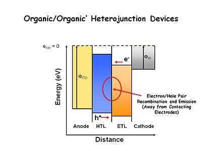
Light emitting thin film system are now built with at least one heterojunction- the interface between two organic layers. The hole transport layer (HTL) is easily oxidized, usually using bis tri aral amines. The electron transport layer (ETL) is easier to reduce and more difficult to oxidize. In electrochemical terms, the HTL should be composed of chemicals that are easy to oxidize and form stable cation radicals, and the ETL should be composed of chemicals that are easier to reduce and form stable radical anions. This results in an energy offset between the two organic layers. Electrons injected into the ETL layer have a large energy barrier to surmount in order to move into the HTL. The holes injected into the HTL have a large energy barrier to move into ETL layer. As a consequence, at low applied fields, the holes and electrons build up at or near the interface. The interface is the site of recombination, which improves device efficiency by keeping recombination from occurring near the electrodes. This was a critically important advancement. | |||
[[category:organic LED]] | |||
<table id="toc" style="width: 100%"> | |||
<tr> | |||
<td style="text-align: left; width: 33%">[[The first OLEDs|Previous Topic]]</td> | |||
<td style="text-align: center; width: 33%">[[Main_Page#Organic_Light_Emitting_Diodes|Return to OLED Menu]]</td> | |||
<td style="text-align: right; width: 33%">[[OLED Charge Mobilities|Next Topic]]</td> | |||
</tr> | |||
</table> | |||
Latest revision as of 10:37, 16 July 2009
| Previous Topic | Return to OLED Menu | Next Topic |
Single-Layer OLEDs Band-Edge Offsets vs. Contact Electrodes
This simplistic energy diagram describes an organic film sandwiched between two contacting electrodes. The anode is indium tin oxide (ITO) and the cathode is aluminum. We assume there is constant vacuum level for all components, although this is not precisely correct. The ITO has a work function represented by the vertical arrow. For clean ITO this is typically 4.7 - 4.8ev. For dirty ITO it can be a low as 4- 4.2ev. The work function for Al is about 4.1ev. The work function difference between the layers allows the aluminum to inject electrons into the organic layer, while the ITO layer injects holes into the organic layer. The work function offset also helps dictate the voltage needed to activate the device.
The energy offset (ΔEh) is the organic layer's ionization potential, defined as the energy required to take an electron out to vacuum. This can be measured with a UV photoelectron spectrometer. There is typically not a good energy match between the ITO bottom contact and the organic layer, causing a small energy barrier that must be overcome in order to inject holes into the organic layer.
The organic layer's electron affinity (EA) is the distance between the vacuum level and the LUMO state, defined as the energy needed to acquire an electron. Cathode materials have a bigger offset (ΔEe) between the work function of the electrode and the electron affinity level. This is the energy barrier for injecting electrons into the organic layer. The same phenomenon occurs in an electrochemical system with a concentrated electrolyte solution, but it can be overcome by setting up an electrical double layer at the interface. The steep potential gradient at the interface makes it possible to get an electron injection regardless of the electrode work function. However in condensed phase environments, which have very low dielectric constants and no added ionic species, these energy levels are significant. Tunneling charges through the energy barriers, or thermionic emission becomes necessary to lower drive voltages.
In early experiments with single crystal anthracene, the charge from the anode and the charge from the cathode did not move at the same rate. In this example, the positive charge electrode which injects holes created a charge carrier that moves faster than the electron carrier. As a result most of the recombination occurs closer to the negative electrode. That is critical problem for display devices because the metal or metal-like electrodes act as an energy sink, and tend to quench emissive states before they give off light. This minimizes the efficiency of the device no matter how much voltage is applied. This scenario was state-of-the-art before two-layer OLEDs were developed.
Organic/Organic’ Heterojunction Devices
Light emitting thin film system are now built with at least one heterojunction- the interface between two organic layers. The hole transport layer (HTL) is easily oxidized, usually using bis tri aral amines. The electron transport layer (ETL) is easier to reduce and more difficult to oxidize. In electrochemical terms, the HTL should be composed of chemicals that are easy to oxidize and form stable cation radicals, and the ETL should be composed of chemicals that are easier to reduce and form stable radical anions. This results in an energy offset between the two organic layers. Electrons injected into the ETL layer have a large energy barrier to surmount in order to move into the HTL. The holes injected into the HTL have a large energy barrier to move into ETL layer. As a consequence, at low applied fields, the holes and electrons build up at or near the interface. The interface is the site of recombination, which improves device efficiency by keeping recombination from occurring near the electrodes. This was a critically important advancement.
| Previous Topic | Return to OLED Menu | Next Topic |

