Difference between revisions of "Major Processes in Organic Solar Cells"
Cmditradmin (talk | contribs) |
Cmditradmin (talk | contribs) |
||
| (55 intermediate revisions by 5 users not shown) | |||
| Line 1: | Line 1: | ||
[[Main_Page#Organic Solar Cells|Return to OPV Menu]] | <table id="toc" style="width: 100%"> | ||
[[ | <tr> | ||
<td style="text-align: left; width: 33%">[[Solar Technologies|Previous Topic]]</td> | |||
<td style="text-align: center; width: 33%">[[Main_Page#Organic Solar Cells|Return to OPV Menu]]</td> | |||
<td style="text-align: right; width: 33%">[[Organic Heterojunctions in Solar Cells|Next Topic]]</td> | |||
</tr> | |||
</table> | |||
Edmond Becquerel (1820-1891) was first to discover the photovoltaic effect. But it was 1954 before the first efficient cell was developed by Chapin, Fuller and Pearson in Bell Labs. They reported a silicon cell with 6% efficiency. | |||
== Comparison of OLEDs and OPVs == | |||
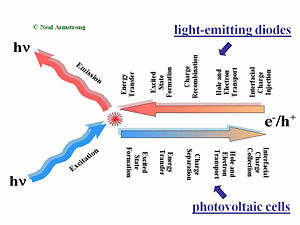
[[Image:led-opvcompared.JPG|thumb|300px|LEDs and photovolataics are opposite processes.]] | [[Image:led-opvcompared.JPG|thumb|300px|LEDs and photovolataics are opposite processes.]] | ||
OLEDs produce light by the injection of charge carriers from the contacting electrodes. Holes typically are injected into the hole-transport layer (HTL) at the bottom transparent contact, and electrons are typically injected at the top metallic contact into the electron transport layer (ETL). These charge carriers migrate toward the center of the device under the influence of the applied field. The rates of charge migration are field-dependent, and dependent upon the mobilities of the holes in the HTL and the electrons in the ETL. In the center of the device, at the HTL/ETL interface, these injected charges (which reside on molecular species as radical cations and radical anions, or polaronic states), must find each other and recombine to form an excited (excitonic) state, from which emission occurs to create light. [[Exciton]] migration, energy transfer to dopants in the OLED, and energy losses occur afterward: the entire process from injection to emission of a photon occurs in less than one microsecond. | |||
An organic photovoltaic cell works in a complementary fashion. Light is absorbed in either of two donor (D) or acceptor (A) layers, creating excitonic states which must diffuse to the D/A interface. Differences in ionization potential and electron affinities of D and A cause these excited states to dissociate into free charge carriers (electrons and holes residing on molecular species). The combination of diffusion and migration of these charge carriers to the collection electrodes, and the harvesting of these charges by these electrodes, produces a current in the external circuit as a specific voltage, the product of which is the power produced by the OPV. | |||
== Energy conversion in OPVs == | |||
===Light Absorption=== | |||
The most efficient OPVs currently have bandgap energies at or above 1.5 eV, which means that they are transparent to much of the near-IR and red regions of the visible wavelength spectrum. These are the regions of maximum solar flux, therefore there has been a great deal of attention focused on creating organic donor and acceptor layers with lower bandgaps, without sacrificing either chemical stability or photopotential (see below). | |||
Inorganic semiconductors are better matched in their bandgap energies to the solar spectrum, but have lower absorptivities than organic materials, requiring thicker absorbing layers, and high purities (and high costs) to insure efficient operation. | |||
Another key difference between OPVs and conventional inorganic solar cells is in the exciton binding energy. In both systems excitons (excited states) are formed upon photon absorption. In inorganic semiconductors the energy required to dissociate these excitons into charge carriers is quite small (a few milli-eVs, easily achieved at room temperature). In organic semiconductors the "exciton binding energy" can be as high as 0.5 eV or higher, requiring the formation of a D/A heterojunction (see below) to provide the internal electrochemical driving force for exciton dissociation to occur. | |||
===Photovoltaic Efficiency=== | |||
[[Image:currentvoltagecurve1.jpg|thumb|300px|Current Voltage curve for a photovoltaic device]] | |||
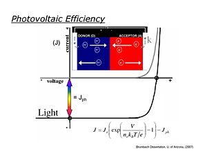
Ideally photovoltaic devices behave like diodes, with dark current/voltage (''J/V'') curves following the Shockley equation. In the dark in the reverse bias direction little measurable current flows, whereas in the forward bias direction, current increases exponentially with applied voltage. When the diode is illuminated, the ''J/V'' curve is ideally shifted down at all potentials by the magnitude of ''J<sub>sc</sub>'', the short-circuit photocurrent. It is in the third quadrant of the ''J/V'' curve (see figure) where power is generated in an external load. | |||
:<math>J=J_0 \left ( exp \left ( \frac {V} {n_0 k_BT/e} \right ) \right ) - J_{ph}\,\!</math> | |||
The maximum power obtainable from an ideal OPV is the product of ''J<sub>sc</sub>'' and the "open-circuit" photovoltage ''V<sub>oc</sub>'' (the voltage obtained for this device at zero current) | |||
:<math>P_{theor} = J_{SC} * V_{OC}\,\!</math> | |||
Real OPVs, however, generate substantially less power, which can be defined where real current/voltage products reach their maximum value: | |||
:<math>P_{max} = J_{max} * V_{max}\,\!</math> | |||
The power conversion efficiency is then defined: | |||
:<math>(P_{max}/P_{solar})*FF\,\!</math> | |||
where P<sub>solar</sub> is the power from the illumination source (sun) and the Fill factor is | |||
:<math>FF = P_{max}/P_{theor}\,\!</math> | |||
Under AM 1.5 solar illumination conditions, most OPVs | |||
*0.4 < ''V<sub>oc</sub>'' < 0.8 volts, | |||
*5 mA/cm<sup>2</sup> < ''J<sub>sc</sub>'' < 15 mA/cm<sup>2</sup>, | |||
*0.4 < ''FF'' < 0.7, leading to power conversion efficiencies of 1-6%. | |||
[[Organic Photovoltaic Fabrication and Test Apparatus]] | |||
[[ | <br clear='all'> | ||
== | == Steps in the Organic Photoelectric Process == | ||
[[Image:Hjsteps.JPG|thumb|400px|Five steps of the excitonic process]] | |||
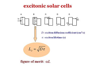
There are five different steps in excitonic solar cells. These 5 steps should also be valid for the organic light emitting diodes-- the fifth step would be the out coupling. The slide shows the energy scheme. | |||
<br clear='all'> | |||
===Light Absorption (exciton formation)=== | |||
[[Image:Opv15-photonabsorption.JPG|thumb|300px|OPV Step 1 Photon absorption]] | |||
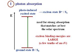
Suppose you have crystalline silicon that absorbs a photon from the solar spectrum, which leads to an excited state. The exciton binding energy is so small that the electron and hole can separate and thus, a current can be produced. However, in an organic material, the absorption of a photon creates a strongly bound exciton. Remember that an exciton is a neutral species. When the electron and the hole are next to one another, the charge is 0 since 1+ + 1- = 0. A current cannot be generated from an exciton. This is why crystalline silicon can perfectly lead to an absorption to the generation of free carriers also known as the band-to-band process. Suppose an exciton is formed on a polythiophene chain. To generate current the exciton must disassociate, meaning the electron and the hole in the exciton must separate, move away from one another, and generate current. | |||
What is most favorable is to have a material that absorbs as intensely and broadly as possible across the solar spectrum. | |||
===Exciton Migration=== | ===Exciton Migration=== | ||
[[Image:opv16_migration.JPG|thumb|300px]] | [[Image:opv16_migration.JPG|thumb|300px|OPV Step 2 Exciton migration to heterojunction]] | ||
Pi- conjugated materials have large binding energies, which is the key difference between an organic solar cell and a crystalline silicon or amorphous silicon solar cell. Excitons must be formed and disassociated to generate a current. | |||
The structure of the organic | The structure of the organic cell includes a component that corresponds to an electron donor and a component that corresponds to an electron acceptor. In order to dissociate, the excitons must reach the interface between those two components. | ||
Excitons travel a certain distance during their lifetime. This distance is called the exciton diffusion length, and is a critical component in device efficiency. To produce current, an exciton must be able to diffuse and reach the interface between the donor and acceptor components during its lifetime. If the interface is 20 nanometers from where the exciton is generated, but during its lifetime the exciton only diffuses 5 nanometers, no current will be produced. If a system has large diffusion lengths but the migration of the exciton takes too long, then the distance between where the exciton is generated and the interface must be reduced, and will result in thinner films. However, thinner films absorb fewer photons. Organic cell engineers must factor in exciton diffusion lengths, exciton lifetimes, and film thickness to design efficient cells. The film must be thick enough to absorb a reasonable amount of photons, but also be thin enough so that the generated excitons can reach the interface efficiently. | |||
This whole process occurs in excitonic solar cells. On the other hand, in organic semi conductors, this exciton part is not dealt with. Actually the very first organic solar cells that has been described in the literature in 1959 by Martin Pope and his workers used a single component called anthracene. The number of charges that were generated was extremely low because when the exciton was formed, it remained bound. Thus, not many charges were separated and little current was generated which leads to a poor efficiency. That is particularly why Ching Tang <ref>C.W. Tang, APL 48, 193 (1985)</ref> made a major advance using heterojunctions that consists of a donor and an acceptor. At step B, the exciton diffuses. | |||
:<math>L_D = \sqrt{D\tau}\,\!</math> | |||
where: | |||
:<math>L_D\,\!</math> is the diffusion length | |||
:<math>D\,\!</math> the diffusion coefficient | |||
:<math>\tau\,\!</math> is the lifetime of the exciton. | |||
As you can see, the equation is an important parameter. The diffusion coefficient D represents how fast the exciton can diffuse within the material or how fast the exciton can hop from molecule to molecule, or from chain segment to chain segment. The larger the diffusion coefficient, the longer the lifetime, which means the further the exciton can go before it decays back to the ground state. It is better if the exciton has a long diffusion length L<sub>D</sub> because it allows the exciton to have a higher chance of reaching the interface with the acceptor within its lifetime. If this process does not occur, no charge will generate and the exciton will decay back to the ground state. This decay will either produce heat, vibrations, or release the photons it once absorbed-- also called photoluminescence. But photoluminescence is not what you want in solar cell. | |||
αL is the figure of merit. It is the product of the diffusion length and the absorption coefficient or the absorbance of the material. The most efficient organic layer would be very absorbing, have a large alpha, and the excitons would have a large diffusion length so that the exciton will have a large probability of finding the interface during its lifetime. | |||
[[Image:opvdesignimprove.jpg|thumb|400px|Light absorption and exciton diffusion. The red line shows the intensity of light as a function of thickness of donor layer. It shows an exponential drop indicating that a thicker layer could absorb all the light. The dashed yellow line indicates the exciton migration before it dies. A thicker layer absorbs more light but the excitons do not make it to the interface to generate a charge. As consequence organic dye layers must be really thin. ]] | |||
<div id="Flash">Exciton Diffusion Animation</div> | |||
In the following Flash simulation the path of an exciton is visualized as you control the thickness of the electon donor layer. You can also experiment with the use of projecting "fingers", a dendritic surface morphology that is being attempted. Note that exciton migration is random diffusion process that does not have a directionality as shown here for instructive purposes. We are only showing the excitons that migrate in a productive direction. | |||
<swf width="500" height="400" >http://depts.washington.edu/cmditr/mediawiki/images/4/42/Excitonmigration.swf</swf> | |||
<br clear='all'> | |||
=== Charge | === Charge Separation (exciton dissociation)=== | ||
[[Image:opv17_chargeseparation.JPG|thumb|300px | |||
This | [[Image:opv17_chargeseparation.JPG|thumb|300px|OPV Step 3 charge separation (exciton dissociation)This diagram shows the events that occur when an exciton reaches the interface between the donor component (D) and the acceptor component (A). ]] | ||
Disassociation, or charge separation, occurs at the interface. Once the electron and the hole have separated, the built in potential cause the electron to drift toward the cathode and the hole to drift toward the anode. If there was no built in potential, the electron and the hole will simply diffuse without any directionality to their motion. | |||
At the interface there are donor molecules or donor polymer chains next to the acceptor molecules or acceptor polymer chains. The lowest energy state is the ground state of the two components. | |||
[[Image:ET_P3HT_to_PCBM.png |thumb|300px|Charge is passed from P3HT to PCBM]] | |||
Suppose that the exciton is formed within the donor. This exciton will be labeled D*, an excited state in the donor. The exciton reaches the interface. There is a state and energy there that corresponds to the exciton energy above the ground state. The exciton transfers its electron to the acceptor, forming a hole on the donor component, and creating the charge transfer state (D<sup>+</sup> A<sup>-</sup>). The + and – charges move away from one another, forming a charge separated state. | |||
To create current, charge transfer (CT) and charge separation (CS) both need to occur. It is possible to have a charge transfer state where the + and the – remain close to each other. However, in order to generate electrical current a full separation of the + and the – is needed. At the CT state, when the hole and electron are next to each other, there is a chance that they will recombine and lead to the ground state. This recombination represents a loss of efficiency in the charge separation process, and is the main reason for low efficiencies of OPVs. | |||
Efficient cells will maximize the rate of charge transfer (k<sub>ct</sub>) and charge separation (k<sub>cs</sub>) and minimize the rate of charge recombination (k<sub>cr</sub>). With those rates, you can also evaluate the Marcus Theory expressions. | |||
===Charge Migration and Collection=== | |||
[[Image:Opv19migration.JPG|thumb|300px|OPV Step 4 Charge Migration]] | |||
During migration the charge move away from the heterojunction interface toward the electrodes. The electron and the hole will be collected efficiently at their respective electrodes, generate a current, and enter the external circuit | |||
Inorganic solar cells can be very efficient because a single inorganic material can be used with an exciton binding energy that is negligible at room temperature. The physics of organic solar cells is very different because the exciton is strongly bound. You need to have an acceptor and donor component with as much interface as possible between them in order that the formed excitons can quickly reach the interface to disassociate. | |||
Once the excitons have disassociated into two separated species, the electron and the hole, they must move efficiently toward the electrodes. Remember that the more you can order your material, in general, the better the mobility will be. The faster the electrons and the holes can move away from each other, the more efficient their separation will be. | Once the excitons have disassociated into two separated species, the electron and the hole, they must move efficiently toward the electrodes. Remember that the more you can order your material, in general, the better the mobility will be. The faster the electrons and the holes can move away from each other, the more efficient their separation will be. | ||
<embed_document width="100%" height="500">http://depts.washington.edu/cmditr/media/type2-heterojunctionOPV.pdf</embed_document> | |||
<br clear='all'> | |||
[[category:organic solar cell]] | [[category:organic solar cell]] | ||
<table id="toc" style="width: 100%"> | |||
<tr> | |||
<td style="text-align: left; width: 33%">[[Solar Technologies|Previous Topic]]</td> | |||
<td style="text-align: center; width: 33%">[[Main_Page#Organic Solar Cells|Return to OPV Menu]]</td> | |||
<td style="text-align: right; width: 33%">[[Organic Heterojunctions in Solar Cells|Next Topic]]</td> | |||
</tr> | |||
</table> | |||
Latest revision as of 10:17, 13 July 2010
| Previous Topic | Return to OPV Menu | Next Topic |
Edmond Becquerel (1820-1891) was first to discover the photovoltaic effect. But it was 1954 before the first efficient cell was developed by Chapin, Fuller and Pearson in Bell Labs. They reported a silicon cell with 6% efficiency.
Comparison of OLEDs and OPVs
OLEDs produce light by the injection of charge carriers from the contacting electrodes. Holes typically are injected into the hole-transport layer (HTL) at the bottom transparent contact, and electrons are typically injected at the top metallic contact into the electron transport layer (ETL). These charge carriers migrate toward the center of the device under the influence of the applied field. The rates of charge migration are field-dependent, and dependent upon the mobilities of the holes in the HTL and the electrons in the ETL. In the center of the device, at the HTL/ETL interface, these injected charges (which reside on molecular species as radical cations and radical anions, or polaronic states), must find each other and recombine to form an excited (excitonic) state, from which emission occurs to create light. Exciton migration, energy transfer to dopants in the OLED, and energy losses occur afterward: the entire process from injection to emission of a photon occurs in less than one microsecond.
An organic photovoltaic cell works in a complementary fashion. Light is absorbed in either of two donor (D) or acceptor (A) layers, creating excitonic states which must diffuse to the D/A interface. Differences in ionization potential and electron affinities of D and A cause these excited states to dissociate into free charge carriers (electrons and holes residing on molecular species). The combination of diffusion and migration of these charge carriers to the collection electrodes, and the harvesting of these charges by these electrodes, produces a current in the external circuit as a specific voltage, the product of which is the power produced by the OPV.
Energy conversion in OPVs
Light Absorption
The most efficient OPVs currently have bandgap energies at or above 1.5 eV, which means that they are transparent to much of the near-IR and red regions of the visible wavelength spectrum. These are the regions of maximum solar flux, therefore there has been a great deal of attention focused on creating organic donor and acceptor layers with lower bandgaps, without sacrificing either chemical stability or photopotential (see below).
Inorganic semiconductors are better matched in their bandgap energies to the solar spectrum, but have lower absorptivities than organic materials, requiring thicker absorbing layers, and high purities (and high costs) to insure efficient operation.
Another key difference between OPVs and conventional inorganic solar cells is in the exciton binding energy. In both systems excitons (excited states) are formed upon photon absorption. In inorganic semiconductors the energy required to dissociate these excitons into charge carriers is quite small (a few milli-eVs, easily achieved at room temperature). In organic semiconductors the "exciton binding energy" can be as high as 0.5 eV or higher, requiring the formation of a D/A heterojunction (see below) to provide the internal electrochemical driving force for exciton dissociation to occur.
Photovoltaic Efficiency
Ideally photovoltaic devices behave like diodes, with dark current/voltage (J/V) curves following the Shockley equation. In the dark in the reverse bias direction little measurable current flows, whereas in the forward bias direction, current increases exponentially with applied voltage. When the diode is illuminated, the J/V curve is ideally shifted down at all potentials by the magnitude of Jsc, the short-circuit photocurrent. It is in the third quadrant of the J/V curve (see figure) where power is generated in an external load.
- <math>J=J_0 \left ( exp \left ( \frac {V} {n_0 k_BT/e} \right ) \right ) - J_{ph}\,\!</math>
The maximum power obtainable from an ideal OPV is the product of Jsc and the "open-circuit" photovoltage Voc (the voltage obtained for this device at zero current)
- <math>P_{theor} = J_{SC} * V_{OC}\,\!</math>
Real OPVs, however, generate substantially less power, which can be defined where real current/voltage products reach their maximum value:
- <math>P_{max} = J_{max} * V_{max}\,\!</math>
The power conversion efficiency is then defined:
- <math>(P_{max}/P_{solar})*FF\,\!</math>
where Psolar is the power from the illumination source (sun) and the Fill factor is
- <math>FF = P_{max}/P_{theor}\,\!</math>
Under AM 1.5 solar illumination conditions, most OPVs
- 0.4 < Voc < 0.8 volts,
- 5 mA/cm2 < Jsc < 15 mA/cm2,
- 0.4 < FF < 0.7, leading to power conversion efficiencies of 1-6%.
Organic Photovoltaic Fabrication and Test Apparatus
Steps in the Organic Photoelectric Process
There are five different steps in excitonic solar cells. These 5 steps should also be valid for the organic light emitting diodes-- the fifth step would be the out coupling. The slide shows the energy scheme.
Light Absorption (exciton formation)
Suppose you have crystalline silicon that absorbs a photon from the solar spectrum, which leads to an excited state. The exciton binding energy is so small that the electron and hole can separate and thus, a current can be produced. However, in an organic material, the absorption of a photon creates a strongly bound exciton. Remember that an exciton is a neutral species. When the electron and the hole are next to one another, the charge is 0 since 1+ + 1- = 0. A current cannot be generated from an exciton. This is why crystalline silicon can perfectly lead to an absorption to the generation of free carriers also known as the band-to-band process. Suppose an exciton is formed on a polythiophene chain. To generate current the exciton must disassociate, meaning the electron and the hole in the exciton must separate, move away from one another, and generate current.
What is most favorable is to have a material that absorbs as intensely and broadly as possible across the solar spectrum.
Exciton Migration
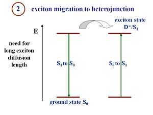
Pi- conjugated materials have large binding energies, which is the key difference between an organic solar cell and a crystalline silicon or amorphous silicon solar cell. Excitons must be formed and disassociated to generate a current. The structure of the organic cell includes a component that corresponds to an electron donor and a component that corresponds to an electron acceptor. In order to dissociate, the excitons must reach the interface between those two components.
Excitons travel a certain distance during their lifetime. This distance is called the exciton diffusion length, and is a critical component in device efficiency. To produce current, an exciton must be able to diffuse and reach the interface between the donor and acceptor components during its lifetime. If the interface is 20 nanometers from where the exciton is generated, but during its lifetime the exciton only diffuses 5 nanometers, no current will be produced. If a system has large diffusion lengths but the migration of the exciton takes too long, then the distance between where the exciton is generated and the interface must be reduced, and will result in thinner films. However, thinner films absorb fewer photons. Organic cell engineers must factor in exciton diffusion lengths, exciton lifetimes, and film thickness to design efficient cells. The film must be thick enough to absorb a reasonable amount of photons, but also be thin enough so that the generated excitons can reach the interface efficiently. This whole process occurs in excitonic solar cells. On the other hand, in organic semi conductors, this exciton part is not dealt with. Actually the very first organic solar cells that has been described in the literature in 1959 by Martin Pope and his workers used a single component called anthracene. The number of charges that were generated was extremely low because when the exciton was formed, it remained bound. Thus, not many charges were separated and little current was generated which leads to a poor efficiency. That is particularly why Ching Tang [1] made a major advance using heterojunctions that consists of a donor and an acceptor. At step B, the exciton diffuses.
- <math>L_D = \sqrt{D\tau}\,\!</math>
where:
- <math>L_D\,\!</math> is the diffusion length
- <math>D\,\!</math> the diffusion coefficient
- <math>\tau\,\!</math> is the lifetime of the exciton.
As you can see, the equation is an important parameter. The diffusion coefficient D represents how fast the exciton can diffuse within the material or how fast the exciton can hop from molecule to molecule, or from chain segment to chain segment. The larger the diffusion coefficient, the longer the lifetime, which means the further the exciton can go before it decays back to the ground state. It is better if the exciton has a long diffusion length LD because it allows the exciton to have a higher chance of reaching the interface with the acceptor within its lifetime. If this process does not occur, no charge will generate and the exciton will decay back to the ground state. This decay will either produce heat, vibrations, or release the photons it once absorbed-- also called photoluminescence. But photoluminescence is not what you want in solar cell.
αL is the figure of merit. It is the product of the diffusion length and the absorption coefficient or the absorbance of the material. The most efficient organic layer would be very absorbing, have a large alpha, and the excitons would have a large diffusion length so that the exciton will have a large probability of finding the interface during its lifetime.
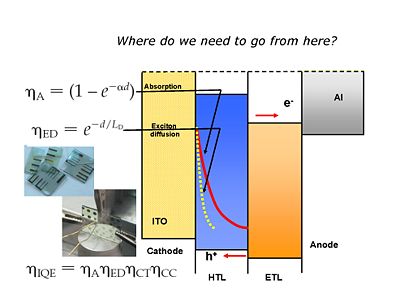
In the following Flash simulation the path of an exciton is visualized as you control the thickness of the electon donor layer. You can also experiment with the use of projecting "fingers", a dendritic surface morphology that is being attempted. Note that exciton migration is random diffusion process that does not have a directionality as shown here for instructive purposes. We are only showing the excitons that migrate in a productive direction.
<swf width="500" height="400" >http://depts.washington.edu/cmditr/mediawiki/images/4/42/Excitonmigration.swf</swf>
Charge Separation (exciton dissociation)
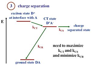
Disassociation, or charge separation, occurs at the interface. Once the electron and the hole have separated, the built in potential cause the electron to drift toward the cathode and the hole to drift toward the anode. If there was no built in potential, the electron and the hole will simply diffuse without any directionality to their motion. At the interface there are donor molecules or donor polymer chains next to the acceptor molecules or acceptor polymer chains. The lowest energy state is the ground state of the two components.
Suppose that the exciton is formed within the donor. This exciton will be labeled D*, an excited state in the donor. The exciton reaches the interface. There is a state and energy there that corresponds to the exciton energy above the ground state. The exciton transfers its electron to the acceptor, forming a hole on the donor component, and creating the charge transfer state (D+ A-). The + and – charges move away from one another, forming a charge separated state.
To create current, charge transfer (CT) and charge separation (CS) both need to occur. It is possible to have a charge transfer state where the + and the – remain close to each other. However, in order to generate electrical current a full separation of the + and the – is needed. At the CT state, when the hole and electron are next to each other, there is a chance that they will recombine and lead to the ground state. This recombination represents a loss of efficiency in the charge separation process, and is the main reason for low efficiencies of OPVs.
Efficient cells will maximize the rate of charge transfer (kct) and charge separation (kcs) and minimize the rate of charge recombination (kcr). With those rates, you can also evaluate the Marcus Theory expressions.
Charge Migration and Collection
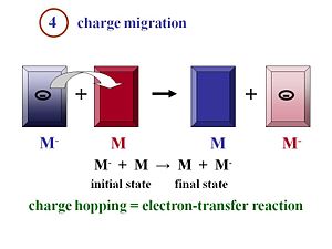
During migration the charge move away from the heterojunction interface toward the electrodes. The electron and the hole will be collected efficiently at their respective electrodes, generate a current, and enter the external circuit
Inorganic solar cells can be very efficient because a single inorganic material can be used with an exciton binding energy that is negligible at room temperature. The physics of organic solar cells is very different because the exciton is strongly bound. You need to have an acceptor and donor component with as much interface as possible between them in order that the formed excitons can quickly reach the interface to disassociate.
Once the excitons have disassociated into two separated species, the electron and the hole, they must move efficiently toward the electrodes. Remember that the more you can order your material, in general, the better the mobility will be. The faster the electrons and the holes can move away from each other, the more efficient their separation will be.
<embed_document width="100%" height="500">http://depts.washington.edu/cmditr/media/type2-heterojunctionOPV.pdf</embed_document>
| Previous Topic | Return to OPV Menu | Next Topic |
- ↑ C.W. Tang, APL 48, 193 (1985)
