Difference between revisions of "Scanning Electron Microscope"
Cmditradmin (talk | contribs) m (→External Links) |
Cmditradmin (talk | contribs) m (→Significance) |
||
| Line 12: | Line 12: | ||
=== Significance === | === Significance === | ||
In addition to producing detailed dramatic pictures that reveal 3D shapes the SEM can be equipped with auxilliary features so it be used for elemental analysis using EDAX and ebeam lithography. | |||
=== Operation === | === Operation === | ||
Revision as of 08:59, 3 November 2011
| Return to Research Tool Menu |
Overview
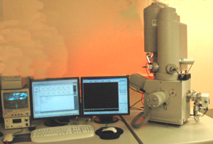
The scanning electron microscope is used to image the surface of a conducting sample by scanning it with a high energy beam of electrons. Some SEMs have additional software enhancements than enable them to focus the beam on a photomask for E-beam lithography or are equipped for focused ion beam (FIB) milling. The SEM is a useful tool for photonics research because it reveals nano-scale surface features and topography that is critical to the performance of multi-layer devices.
Significance
In addition to producing detailed dramatic pictures that reveal 3D shapes the SEM can be equipped with auxilliary features so it be used for elemental analysis using EDAX and ebeam lithography.
Operation
Part 1 Tour and Sample Preparation
Part 2 Loading the Sample
Part 3 Setting the Working Distance
Part 4 Lens Alignment and Stigmation
Part 5 Moving the Stage and Imaging
Part 6 Changing the Sample and Shutdown
