Difference between revisions of "OLED Charge Mobilities"
Cmditradmin (talk | contribs) |
Cmditradmin (talk | contribs) |
||
| (42 intermediate revisions by 4 users not shown) | |||
| Line 1: | Line 1: | ||
[[Main_Page# | <table id="toc" style="width: 100%"> | ||
<tr> | |||
<td style="text-align: left; width: 33%">[[Organic/Organic Heterojunctions in OLEDs|Previous Topic]]</td> | |||
<td style="text-align: center; width: 33%">[[Main_Page#Organic_Light_Emitting_Diodes|Return to OLED Menu]]</td> | |||
<td style="text-align: right; width: 33%">[[Organic Heterojunctions|Next Topic]]</td> | |||
</tr> | |||
</table> | |||
==Fundamentals of Charge Transport in Organic Solids== | ==Fundamentals of Charge Transport in Organic Solids== | ||
[[Image:Transport.png|thumb|400px|Crystalline and amorphous organic conductors compared ]] | |||
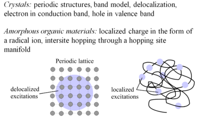
The concept of charge transport was developed first for crystals. Crystals have period structures, the band model applies, and there is delocalization of electrons in the electron conduction band and holes in the valence band. This is the case with doped silicon. | |||
Amorphorous organic materials have charge localized in the form of radical ions which move by interstitial hopping (hopping from molecular site to molecular site). This process is intrinsically less efficient than in crystalline inorganic semiconductors, which is reflected in the lower mobility of charge carriers. | |||
Hole conduction and electron conduction occur in opposite directions as a result of an applied electric field. They do not occur at the same rate. In general, electron conduction is a slower process than hole transport. | |||
[[Image:OLED6_transportrates.JPG|thumb|300px|Comparative Charge Mobilities]] | [[Image:OLED6_transportrates.JPG|thumb|300px|Comparative Charge Mobilities]] | ||
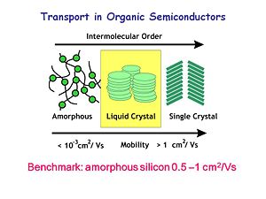
In the early days of OLED research, there was an amorphous organic state, the liquid crystal state and the single crystal state. The benchmark mobility for amorphous silicon is 0.5 x 10<sup>-1</sup> cm<sup>2</sup>/Vs. Charge mobility is measured as the flux of charge in one square centimeter per volt per second. Most organic materials have charge mobility between 10<sup>-3</sup> cm<sup>2</sup>/Vs and 1 cm<sup>2</sup>/Vs. These mobilities limit how thick an organic device can be. OLEDs are optimized at low thicknesses because of these low mobilities. Over the last two decades, materials with higher mobilities have been developed. For example, the mobility of single crystal rubrene is around 10<sup>-15</sup> cm<sup>2</sup>/Vs. There are also liquid crystalline systems which exhibit good charge mobilities along the stacking axis. These developments show that organic materials have the potential to reach high mobilities. | |||
See also [[Charge Carrier Mobility]] | |||
==Transfer Mobility Experiments== | |||
[[Image:Tof.png|thumb|300px|Time of flight measurement using an N<sub>2</sub> laser, 337 nm, 6ns pulse ]] | |||
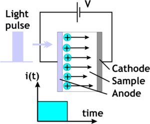
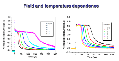
To measure mobility you create a thick film of the organic material, place it over the top of a transparent electrode and place a collection electrode on the side. Then fire a laser at a wavelength that will photogenerate charge carriers. There may be a sensitizer, or the laser can be tuned to one of the absorption bands for the organic material. Suppose you use a nitrogen laser in the UV with a short pulse length which launches a sheet of charges into the organic layer. Then we measure the amount of time it takes for the charges to arrive at the collection electrode and then fall off. This is the time of flight (TOF)<ref>http://www.springerlink.com/content/77n555033k56834m/</ref>. The vertical axis is the compensation current in the external circuit. We measure the transit time measured at the inflection point of the curve. Notice that as you increase the voltage of the system, the transit time goes down. | |||
:<math>\epsilon = \mu E = \mu \frac {V} {L}\,\!</math> | |||
:<math>\tau = \frac {L} {\epsilon}= \frac {L^2} {\mu V}\,\!</math> | |||
:<math>R= 10^2 - 10^4 \Omega, C= 10pf, RC <<\tau \,\!</math> | |||
Electron mobilities are therefore field dependent. It is best to have non-dispersive transport in which charges start as a sheet of charges and then move across the material as a sheet resulting in a very well defined transition. If the motion of the charges is more randomized, if there is disorder in the solid and a lots of traps, then you get a less clear transition point. This is dispersive transport. | |||
[[Image:Field-Tdependence.png |thumb|400px|Electron mobility Field and Temperature Dependence]] | |||
The second series of plots shows that the process is temperature dependent, indicating that it is an activated process. This is activation of a charge from one molecular center, up and over a barrier and into another molecular center. This is similar to the problem of electron transfer that Marcus first described, and it is dependent on the internal and external reorganization energy that involves charge transfer from one species to another. It can be described in much the same manner that Marcus first described homogeneous electron transfer. | |||
<br clear="all"> | |||
==The Disorder Formalism (Bassler and Borsenberger)== | |||
[[Image:OLED6_disorderformalism.jpg|thumb|400px|Transport occurs by hopping through a manifold of localized states with energetic and positional disorder.]] | |||
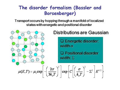
There have been many efforts to formally describe the process of charge transport. The disorder formalism of Bassler and Borsenberger best describes what we see. Transport occurs by hopping through a manifold of localized states that are energetically and positionally disordered. This describes transport for most organic systems. Mobility can be expressed in terms of intrinsic mobility and a Boltzman-like expression that accounts for the energy barriers and the degree of disorder in the system. This accounts for the temperature dependence and the field dependence of transfer. | |||
:<math>\mu(E,T)= \mu_0 exp \left [ - \left (\frac {2 \sigma} {3k_{BT}} \right)^2 \right ] exp \left \lbrace C \left [ \left ( \frac {\sigma} {k_BT} \right )^2 - \sum^2 \right ] E^{1/2} \right \rbrace\,\!</math> | |||
[[Image:OLED6_fieldependance.jpg|thumb|400px|This graph shows the mobility of charge carriers in several transport materials as a function of the applied voltage. The mobility is a function of the square root of the field. These show a charge mobility of less than 10<sup>-4</sup> and for some systems it can get worse than that.]] | |||
<br clear="all"> | <br clear="all"> | ||
[[Image:OLED6_disorder-dipolar.JPG|thumb|400px|Random distribution of dipoles generates fluctuations in electrostatic potential.]] | |||
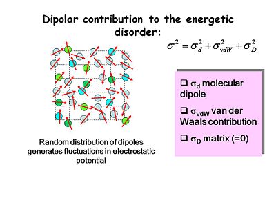
There | There are several contributions to energetic disorder including molecular dipole, Van der Waals or dispersive interactions, and matrix interactions. Random distribution of dipoles generates fluctuation in electrostatic potential because local dipole fields could either help or hinder the movement of charge from one system to another. Most good OLED materials are non-polar and have no intrinsic local dipoles. | ||
<br clear="all"> | |||
==Hole and Electron Mobility in Non-Crystalline Materials== | ==Hole and Electron Mobility in Non-Crystalline Materials== | ||
Here are actual mobilities for non- | [[Image:OLED6_noncrystalinemobility.JPG|thumb|400px|Hole and Electron Mobility in Non-crystalline materials]] | ||
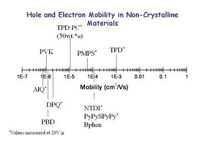
Here are actual mobilities for non-crystalline materials. Triphenyldiamne (TPD) is a bis arylamine which at the time was one of the better compounds with a mobility of 10<sup>-3</sup>. A 50% TPD/polycarbonate solution (TPD:PC) results in a mobility drop of two orders of magnitude. Poly vinyl carbazol (PVK) has been used extensively, but its mobility is poor. Aluminu quinalate (AlQ), DPQ and PBD are electron transporter and emissive materials which also have low mobility. If you make an OLED with one of these hole transport materials and another electron transport material there will be an asymmetry in their rates. | |||
[[category:organic LED]] | |||
[[category:transport properties]] | |||
== References == | |||
<references/> | |||
<table id="toc" style="width: 100%"> | |||
<tr> | |||
<td style="text-align: left; width: 33%">[[Organic/Organic Heterojunctions in OLEDs|Previous Topic]]</td> | |||
<td style="text-align: center; width: 33%">[[Main_Page#Organic_Light_Emitting_Diodes|Return to OLED Menu]]</td> | |||
<td style="text-align: right; width: 33%">[[Organic Heterojunctions|Next Topic]]</td> | |||
</tr> | |||
</table> | |||
Latest revision as of 14:26, 7 July 2010
| Previous Topic | Return to OLED Menu | Next Topic |
Fundamentals of Charge Transport in Organic Solids
The concept of charge transport was developed first for crystals. Crystals have period structures, the band model applies, and there is delocalization of electrons in the electron conduction band and holes in the valence band. This is the case with doped silicon. Amorphorous organic materials have charge localized in the form of radical ions which move by interstitial hopping (hopping from molecular site to molecular site). This process is intrinsically less efficient than in crystalline inorganic semiconductors, which is reflected in the lower mobility of charge carriers.
Hole conduction and electron conduction occur in opposite directions as a result of an applied electric field. They do not occur at the same rate. In general, electron conduction is a slower process than hole transport.
In the early days of OLED research, there was an amorphous organic state, the liquid crystal state and the single crystal state. The benchmark mobility for amorphous silicon is 0.5 x 10⁻¹ cm2/Vs. Charge mobility is measured as the flux of charge in one square centimeter per volt per second. Most organic materials have charge mobility between 10-3 cm2/Vs and 1 cm2/Vs. These mobilities limit how thick an organic device can be. OLEDs are optimized at low thicknesses because of these low mobilities. Over the last two decades, materials with higher mobilities have been developed. For example, the mobility of single crystal rubrene is around 10-15 cm2/Vs. There are also liquid crystalline systems which exhibit good charge mobilities along the stacking axis. These developments show that organic materials have the potential to reach high mobilities.
See also Charge Carrier Mobility
Transfer Mobility Experiments
To measure mobility you create a thick film of the organic material, place it over the top of a transparent electrode and place a collection electrode on the side. Then fire a laser at a wavelength that will photogenerate charge carriers. There may be a sensitizer, or the laser can be tuned to one of the absorption bands for the organic material. Suppose you use a nitrogen laser in the UV with a short pulse length which launches a sheet of charges into the organic layer. Then we measure the amount of time it takes for the charges to arrive at the collection electrode and then fall off. This is the time of flight (TOF)[1]. The vertical axis is the compensation current in the external circuit. We measure the transit time measured at the inflection point of the curve. Notice that as you increase the voltage of the system, the transit time goes down.
- <math>\epsilon = \mu E = \mu \frac {V} {L}\,\!</math>
- <math>\tau = \frac {L} {\epsilon}= \frac {L^2} {\mu V}\,\!</math>
- <math>R= 10^2 - 10^4 \Omega, C= 10pf, RC <<\tau \,\!</math>
Electron mobilities are therefore field dependent. It is best to have non-dispersive transport in which charges start as a sheet of charges and then move across the material as a sheet resulting in a very well defined transition. If the motion of the charges is more randomized, if there is disorder in the solid and a lots of traps, then you get a less clear transition point. This is dispersive transport.
The second series of plots shows that the process is temperature dependent, indicating that it is an activated process. This is activation of a charge from one molecular center, up and over a barrier and into another molecular center. This is similar to the problem of electron transfer that Marcus first described, and it is dependent on the internal and external reorganization energy that involves charge transfer from one species to another. It can be described in much the same manner that Marcus first described homogeneous electron transfer.
The Disorder Formalism (Bassler and Borsenberger)
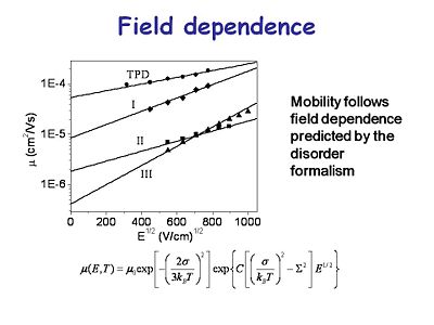
There have been many efforts to formally describe the process of charge transport. The disorder formalism of Bassler and Borsenberger best describes what we see. Transport occurs by hopping through a manifold of localized states that are energetically and positionally disordered. This describes transport for most organic systems. Mobility can be expressed in terms of intrinsic mobility and a Boltzman-like expression that accounts for the energy barriers and the degree of disorder in the system. This accounts for the temperature dependence and the field dependence of transfer.
- <math>\mu(E,T)= \mu_0 exp \left [ - \left (\frac {2 \sigma} {3k_{BT}} \right)^2 \right ] exp \left \lbrace C \left [ \left ( \frac {\sigma} {k_BT} \right )^2 - \sum^2 \right ] E^{1/2} \right \rbrace\,\!</math>
There are several contributions to energetic disorder including molecular dipole, Van der Waals or dispersive interactions, and matrix interactions. Random distribution of dipoles generates fluctuation in electrostatic potential because local dipole fields could either help or hinder the movement of charge from one system to another. Most good OLED materials are non-polar and have no intrinsic local dipoles.
Hole and Electron Mobility in Non-Crystalline Materials
Here are actual mobilities for non-crystalline materials. Triphenyldiamne (TPD) is a bis arylamine which at the time was one of the better compounds with a mobility of 10-3. A 50% TPD/polycarbonate solution (TPD:PC) results in a mobility drop of two orders of magnitude. Poly vinyl carbazol (PVK) has been used extensively, but its mobility is poor. Aluminu quinalate (AlQ), DPQ and PBD are electron transporter and emissive materials which also have low mobility. If you make an OLED with one of these hole transport materials and another electron transport material there will be an asymmetry in their rates.
References
| Previous Topic | Return to OLED Menu | Next Topic |
