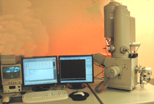
Scanning Electron Microscope
| Return to Research Tool Menu |
Overview
The scanning electron microscope is used to image the surface of a conducting sample by scanning it with a high energy beam of electrons. The SEM is a useful tool for photonics research because it reveals nano-scale surface features and topography that is critical to the performance of multi-layer devices. SEM produces dramatic pictures that reveal 3D shapes and shadows.
Significance
Some SEMs have additional software enhancements than enable them to focus the beam on a photomask for E-beam lithography or are equipped for focused ion beam (FIB) milling. SEM can be equipped with attachments so it be used for elemental analysis using Energy Disspersive X-ray spectroscopy EDAX.
Operation
Part 1 Tour and Sample Preparation
Part 2 Loading the Sample
Part 3 Setting the Working Distance
Part 4 Lens Alignment and Stigmation
Part 5 Moving the Stage and Imaging
Part 6 Changing the Sample and Shutdown
