Optical Networks
| Previous Topic | Return to Organic Photonics Applications Menu | Next Topic |
Introduction to Optical Networks
An optical network can be thought of as rings that are connected together at various distances (1-100s kms)
Optical fiber sets the rules
All optical networking is made possible by the development of optical fibers by AT&T and Corning in the late 1960s. This graph shows attenuation as a function of wavelength. At the most common optical communication wavelength of 1550 nm the attenuation is as low .2 decibels per km. That is only a few percent of loss. Imagine a piece of glass a mile long that is perfectly clear. This was a great achievement for materials science because when they started they were working with losses of decibels per meter. By understanding what led to the loss in fiber they were able to optimize materials and fabrication techniques. The labels across the top indicate important telecommunication wavelengths. 1310 nm was for a long time the most important wavelength because it is the lowest dispersion point where the lease amount of spreading of the light waves happens.
The S, C and L lines in the 1550 nm range is much more important today because it is the range of the erbium doped fiber amplifier (EDFA) which can boost the signal along thousands of kms without having to be turned back into electricity. This is also the range where there is low attenuation.
http://en.wikipedia.org/wiki/Optical_amplifier
Basic optical fiber link
The most elemental optical network requires a transmitter, connected to a receiver with an optical fiber. The transmitter (Tx) can be a directly modulated source such as a laser that is turned on and off. Or it can be an externally modulated (at digital rates up to 40 Gigabits/sec) by passing a constant laser beam through a modulating device. At the end of the fiber link the neat square waves may become spreadout. They are then read by a receiver (Rx) which is a semiconductor detector that operates at high speed and high sensivity (microwatt level). In areas that have local fiber to the home have this very basic configuration over short distances without amplification.
Advanced optical network: dense wavelength division multiplexing A long distance optical network uses dense wavelength division multiplexing. Mux is an optical multiplexer that combines the separate transmitters onto a single optical fiber; demux does the inverse operation.
Transmitters are different wavelengths, narrowly spaced from one another (~ 1 nm) on a standard grid; transmitter can consist of a cw laser + EO modulator
EDFA is an erbium doped fiber optical amplifier that simultaneously amplifies all wavelengths without causing noise or crosstalk. Nature was very kind to provide fiber that is very clear at 1550 nm, however after a 20-30 kms the signal still needs to be regenerated. This could be done by turning the light back into electricity, amplifying this signal and then regenerating the modulated light.
Erbium doped devices have the ability to directly amplify light by 100-1000 times and with simultaneous different wavelengths and without interference. This expands the range of fiber signals to hundreds or thousands of kms.
OADM is an optical add-drop multiplexer is essentially a traffic controller that allows signals to be dropped and added along the way.
The demux is able to separate wavelengths to different receivers. This means that additional bandwidth can be achieved by adding additional wavelengths. This can be done without digging up and replacing fiber which is still the most expensive part of the system.
Passive optical network architecture
The passive optical network system is beginning to be deployed in Japan is able to combine. At the central office the OLT – optical line terminal is able to combine various signals such as broadcast TV (1550nm), phone (1490nm) or two way data (1310nm) into a single optical fiber. An optical splitter distributes light from the single fiber into many individual fibers going to each customer premise where is separated into the various electrical signals at the ONU – optical network unit . The OLT equipment can be allowed to be very expensive because it is centrally located but the ONU must be very inexpensive to make the economics of the system feasible. This where EO polymers have real possibilities.
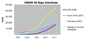
The bandwidth of fiber is enormous, far higher than coaxial cable or twisted pair phone lines. There are many application for electro-optics. At the 40 Gbps area the demand is rapidly increasing.
Defense:
- Phased-array antennas
- Fiber gyroscopes
- A-to-D converters
Commercial:
- OC-768 (40Gbps) optical networking
- Optical interconnects
- Fiber-to-the-home, CATV
- Integration with thin-film optoelectronics
Electro Optical devices
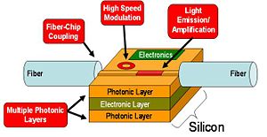
Electoroptical materials and new nanotechnology methods make it possible to build new devices that are critical to the telecommunications and computing system.
Modulators
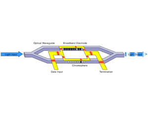
Modulators and Detectors- use electrical field to influence optical materials, or optical field to control an electrical field.
- Second order nonlinear optical materials
- Electro-absorptive materials(InP)
- Crystalline and liquid crystalline materials
- SiGe photodetectors
The electrical or optical signal feeds into a modulator, then into a waveguide, and then back to a photodetector, leading to an electrical format in a logic cell.
We must be able must be able to seamlessly handle electronic (electron) and photonic (photons or optical) signals including converting between the two signal types.
How do we interconvert electronic and photonic signals? This brings us to the concept of electro-optic materials. Basically, we are going to use the simultaneous interaction of electrical and optical signals with the electron distribution of a material to provide a means of these two types of signal to communicate. This entails the concept of Molecular & Macroscopic Polarizability
Flash simulation of wave interference
Waveguides
Waveguides- These components carry light.
- Silica (long haul)
- Graded Index Polymers (short haul)
- Silicon nanophotonic (chipscale transmission)- the most popular recent discovery
- Silver nanophotonic/plasmonic (chipscale)
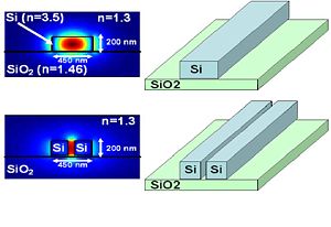
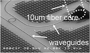
A silicon waveguide for telecommunications wavelength has a diameter of 10 micrometers, a human hair is 250 microns. Because silicon has a high index of refraction, waveguides can be made very small and they can light around a right angle bend. Silica (glass) fibers could not make this bend without disrupting the transmission. A silicon waveguide can be as small as 10 microns down to 200-250 nanometers. It can be fabricated on the same equipment as CMOS.
In a normal optical fiber the light intensity is concentrated in the middle of the guide. But if you cut a 70nm slot down the middle of the waveguide the light intensity is maximized inside the slot with tremendous amplification.
Normally optical devices must not be smaller than the wavelength of the light they carry. However a new development is called sub-wavelength photonics.Mahel Lipson at Cornell , and Axel Scherer at Caltech and his student Michael Hochberg have been able to develop this technique. Take silica fiber and irradiate an array waveguide grating and couple that light into a silicon nanophotonic waveguide. Then fill the waveguide slot with an organic EO material for active control of light.
Optical waveguides
A slab type optical waveguide has a core material that has an index of refraction ncore that is higher than the cladding nclad. Light launched into core will propagate by total internal reflection. A channel waveguide has reflection in all directions around the core.
Maxwells wave equation:
- <math>{\frac {\partial E_x(y)} {\partial y^2} = [\beta ^2 - n^2_(y) K^2_0] E_x (y)}\,\!</math>
You can solve for β with a transcendental equation:
- <math>(k^2_{core} - \beta ^2_m)^{1/2}d- 2\phi = \pi m\,\!</math>
- <math>k=2\pi n/\lambda\,\!</math>
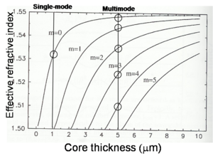
β is the propagation constant which determines if light will be propagated in the waveguide
The graph show contours of beta at various thicknesses. The larger the waveguide the more modes that are possible. Multiple modes will spread out due to the differences in the speed of propagation of the waves. Therefore the majority of all long distance optical network (over 1km distance) uses single mode fiber which is very small (<2 mum)
Ring resonator
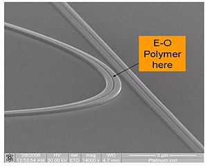
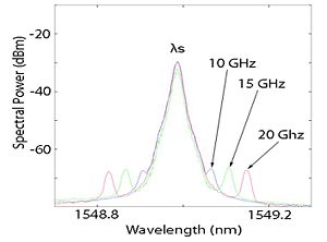
A resonator is a device that acts a filter in an optical circuit using constructive interference. A ring resonator will only propagate certain wavelengths of light determined by the circumference of the ring and by the index of refraction of the material. If you apply a voltage to the EO material you will change its index of refraction, an thereby you can control the wavelength of light that is coupled into the ring. A ring gives you the capability of building a welding switch that can couple certain wavelength of light over to another waveguide. So we can electronically control the transfer of light from one waveguide to another. You can electronically control the color of light that is coupled, this is known as wavelength division multiplexing.
In telecommunications this is the dominant technique for increasing density of throughput in optical systems. You can distribute information over different wavelengths. If you have 10 wavelengths you can carry 10 times as much information. You can also encode electrical information about a given color while it is in the ring because of the elecro-optical effect.
Reconfigurable Optical Add Drop Multiplexer
This is the result from a paper in the Journal of lightwave technology submitted by Boeing, UW and Caltech, showing a 4x 4 x4 reconfigurable optical addrop multiplexor. By changing the electrical fields on EO materials we can control the routing of optical paths, the color of the routed light, and the electrical coding of that light. This could be used in Boeing AWAC aircraft. This would move hundreds of pounds of cables onto a single card.
Waveguide Power advantages
A waveguide concentrates a lot of optical field in a small dimension thus providing the same power concentration as you would get with a high power military grade laser. This allows you to use NLO effects that would normally require a much more powerful source.
The concentration of electrical and optical fields in silicon photonics permits millivolt electro-optic modulation; less than microwatt optical rectification (photodetection without the need to excite electrons from the ground state thus eliminating some noise sources in photodetection), and microwatt all-optical modulation and switching (optical computing). In the latter two cases, the bandwidth is on the order of 10 THz
See Hochberg [1]
Figures of Merit
- Optical pump power less than1 mW (3 x 10⁶ V/m)
- 1/3 power in organic NLO cladding
- χ(3) = 6-7 x 10-21 (m/V)2
- Modulation to 10 THz
Array waveguide grating (AWG)
The array waveguide is a very successful electro-optical device which works on the principle of interference.
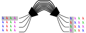
The array waveguide is essentially a multistage, multi cross-connect wavelength coupler. The delay lines between the two sides cause different phase shifts for different wavelength and therefore different wavelengths from one input appear at different outputs.
By coupling each input to all outputs and controlling the characteristics of the coupling, a wavelength at any input can be coupled to a selected outputs. This structure is also known as an MxN multiplexer (or demultiplexer is used in the opposite direction).
Other names found in the literature: Phase array, phaser, Dragone router.
Decibels
Decibels is a log10 scale.
- <math>Loss(db) = -10 log_{10}\left ( \frac {P_{out}} {P_{in}}\right )\,\!</math>
Hint: Just remember that 3 db is equivalent to 50 percent transmission. Then you can build up the ratios logarithmically from there; 6db is 25%, 12 db is 5%.
| Previous Topic | Return to Organic Photonics Applications Menu | Next Topic |
- ↑ M. Hochberg et al., “All-Optical Modulator in Si with THz Bandwdith,” Nature Materials, 5, 703-709 (2006)


