The First OLEDs
Return to OLED Menu | Next Topic
The first OLEDs were green as seen in this early example from the University of Arizona. The image on the right is so bright that is appears white.
The First (“Heroic”) Experiments to Generate Light From Organic Materials:Top and Bottom Electrodes/Rectifying Junctions
The first experiments to generate light from organic materials can be traced back to the late 1950s and early 1960’s at places like RCA.
See W. Helfrich & W.G. Sneider Phys. Rev. Lett. 14(7), 229 (1965)
People would take highly purified anthracene and cut it very fine, approximately 5mm thick. They would connect these to electrodes and apply between 100 and 1000 volts. If the system did not short there would be light emission. Often there would be a lightning bolt like discharge and you produce graphite instead of light.
<embed_document width="55%" height="400">http://depts.washington.edu/cmditr/media/OLED4_firstexperiments.pdf</embed_document>
Next they brought the thickness down to 50 microns and used a saw emission from a semitransparent gold electrode. How is light generated? At the anode there is the removal of an electron to create a cation radical state. At the cathode is the addition of an electron to create the anion radical state. These charges need to hop through the organic crystal in order to meet each other somewhere near the center of the device. They undergo an electron transfer between this reduced donor and the oxidized receptor. There is enough excess free energy generated to create the emissive state of anthracene. The key piece is that in the early devices the rate of transport of the positive cation radical or hole state and the transport of the electron rich state where not equal so the recombination occurred near one of the contacting electrodes. This proves to be a real problem for the efficiency of the device.
The First “Practical” Organic Light Emitting Diodes
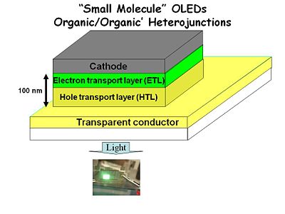
The first practical OLEDs was in the late 1980’s by Ching Tang and Andy Van Slyke at Kodak. This was revolution for the technology. They started with a glass or plastic substrate with a transparent conductor such as indium tin oxide which can be highly doped and be highly conductive yet maintain transparency in the visible wavelength region. They deposited a hole transport layer typically some tri aral amine or in the early versions a polymer called poly vinyl carbazol; something that is easily oxidized at this transparent conductor.
Next we add an electron transport layer and the total thickness has been reduced down to 100 nm. This was a technological advance because you were no longer having to slice single crystal anthracene really thin with a razor knife instead you are vapor depositing molecules in a vacuum system on top of this transparent conductor. This also solved another problem. When you deposit two successive layers there are fewer pin holes that create a dead short circuit between the anode and cathode.
Finally the top electrode is something like aluminum, magnesium, silver alloy or even an electropositive metal such as calcium. The hole transparent layer was a spin coated polymer. This produced about 15 candelas per square meter. A typical CRT computer screen operates with 100-200 candelas per square meter. So this was a dim but visible light. Aluminum tris quinalate was used as both the electron transport and emissive layer.
See C.W. Tang and S.A. VanSlyke Appl. Phys. Lett. 51, 913(1987) C.W. Tang, U.S. Patent # 4,356,429 (1980)
Vacuum deposition enabled thin electron transport layer
Hole transport layer was spin-coated polymer: 10 – 20 V, 15cd/m2 brightness
All vacuum device: 10 – 20 V, 100 cd/m2 using Alq3 emission layer
