Difference between revisions of "Chemical Vapor Deposition"
Jump to navigation
Jump to search
Cmditradmin (talk | contribs) m (→Background) |
Cmditradmin (talk | contribs) m (→Background) |
||
| Line 5: | Line 5: | ||
=== Background === | === Background === | ||
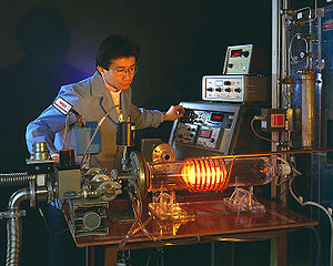
[[Image:750px-CVD Reaction Chamber - GPN-2000-001466.jpg|thumb|300px|Chemical Vapor Deposition Apparatus ]] | |||
Chemical Vapor Deposition is a common technique for apply thin films to electronic devices. Chemical reagents are supplied as gases into chamber and allowed to react or decompose at the surface of as substrate and form a new substance. | Chemical Vapor Deposition is a common technique for apply thin films to electronic devices. Chemical reagents are supplied as gases into chamber and allowed to react or decompose at the surface of as substrate and form a new substance. | ||
<br clear='all'> | |||
=== Significance === | === Significance === | ||
Revision as of 09:29, 20 June 2011
| Return to Research Tool Menu |
Background
Chemical Vapor Deposition is a common technique for apply thin films to electronic devices. Chemical reagents are supplied as gases into chamber and allowed to react or decompose at the surface of as substrate and form a new substance.
Significance
CVD is a high volume, high purity process that can be conducted with low vacuum. The flow rate of the gases can be used to efficiently support the stoichiometry of the reaction.
<swf width="600" height="400">images/6/62/Cvd.swf</swf>
