Difference between revisions of "Scanning Electron Microscope"
Jump to navigation
Jump to search
Cmditradmin (talk | contribs) m (→Operation) |
Cmditradmin (talk | contribs) m (→Overview) |
||
| Line 1: | Line 1: | ||
=== Overview === | === Overview === | ||
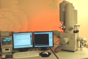
[[Image:Sirion_sem.png|thumb|300px|]] | [[Image:Sirion_sem.png|thumb|300px|]] | ||
The scanning electron microscope is used to image the surface of a conducting sample by scanning it with a high energy beam of electrons. Some SEMs | The scanning electron microscope is used to image the surface of a conducting sample by scanning it with a high energy beam of electrons. Some SEMs have additioanal software enhancements than enable them to focus the beam on a photomask for E-beam lithography or are equipped for focused ion beam (FIB) milling. | ||
See Wikipedia on [http://en.wikipedia.org/wiki/Scanning_electron_microscope Scanning Electron Microscope] | See Wikipedia on [http://en.wikipedia.org/wiki/Scanning_electron_microscope Scanning Electron Microscope] | ||
=== Operation === | === Operation === | ||
Revision as of 12:47, 14 October 2009
Overview
The scanning electron microscope is used to image the surface of a conducting sample by scanning it with a high energy beam of electrons. Some SEMs have additioanal software enhancements than enable them to focus the beam on a photomask for E-beam lithography or are equipped for focused ion beam (FIB) milling.
See Wikipedia on Scanning Electron Microscope
Operation
Video in production
Training Manual for Sirion SEM[1]
Training Video on Hitachi 3500H SEM at GT MiRC
