Difference between revisions of "Materials Processing and Fabrication"
| Line 6: | Line 6: | ||
</table> | </table> | ||
==Polymer Manufacturing into Devices== | |||
=== Polymer waveguide fab: RIE === | |||
[[Image:RIE.png|thumb|300px|Reactive Ion Etching of a polymer with applied mask]] | |||
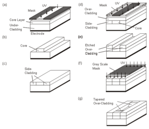
Reactive Ion Etching (RIE) is used to convert a slab waveguide into a channel waveguide. | |||
#First a slab is prepared with a core layer (higher index of refraction) is placed on a polymer undercladding on a silicon substrate. | |||
#A metallic photo mask is applied to protect the core material. | |||
#A plasma of oxygen is used to eat away the unmasked portion of the polymer. | |||
#The metalic mask is removed and the ribbon of core material is fully encased with overcladding. | |||
=== Sol-gel waveguide fabrication === | |||
[[Image:Sol_gel_production.png|thumb|300px|Sol-gel waveguide fabrication (including gray scale masking)]] | |||
This technique builds a complex sol-gel waveguide using completely wet techniques (no vacuum required). Direct illumination by UV through a mask is able to fix portions of the core in place, while unfixed portions are washed away. A series of steps like this can be used to build a complex device. | |||
=== Polymer waveguide fab: Results === | |||
[[Image:Polymer_waveguide_SEM.png|thumb|300px|Etched polymer waveguide]] | |||
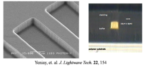
The company Photon X has commercialized the polymer waveguide process. The SEM (5micron line shown) shows very smooth sidewalls from a high quality etching process. Walls can only have roughness of 40-50 nm before there is significant optical loss. The polymer waveguide shows excellent light transmission through a 4 mum x 4 mum waveguide core that has been designed to couple very well with an optical fiber. | |||
See Yeniay <ref>Yeniay, et. al. J. Lightwave Tech. 22, 154</ref> | |||
<br clear='all'> | |||
=== Polymer waveguide fab UV curing === | |||
[[Image:Waveguide_uvcuring.png|thumb|300px|Two waveguides produced by UV photo curing process]] | |||
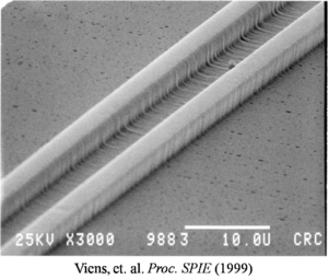
This waveguide is created using the same UV curing process that is used with sol-gels. This shows two waveguides very close to each other. The channel is very difficult to control using photo etching process. The SEM shows a little cross striation but overall very good quality results. | |||
See Viens 1999 <ref>Viens, et. al. Proc. SPIE (1999)</ref> | |||
<br clear='all'> | |||
=== Polymer athermal Array Waveguide Gradiant AWG filter === | |||
[[Image:Fibertofiber_transmission.png|thumb|300px| Measured fiber-to-fiber transmission spectra]] | |||
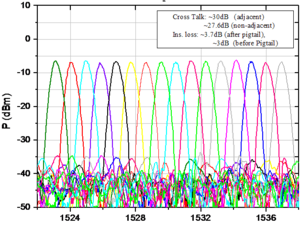
An array waveguide gradiant is used to separate out wavelengths into separate ports. To characterize the device you shine a variety of wavelengths through the device simulating various information carriers and then measure the output from each port. The fluorinated polymer device was able to achieve these results: | |||
*Insertion loss: 3 dB | |||
*Adjacent crosstalk: -30dB | |||
*Non-adjacent crosstalk: -28 dB | |||
This passive polymer technology is being used to connect servers (interconnects) in server forms over very short distances with tremendous data rates. | |||
<br clear='all'> | |||
[[Image:Temperature_dependence.png|thumb|300px|]] | |||
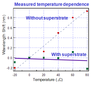
An athermal device performs equally well at different temperatures without temperature control. | |||
Wavelength Temperature Dependence dλ/dt : | |||
*without superstrate: 12pm/ °C | |||
*with superstrate: - 0.5pm/ °C | |||
See Gao 2002 <ref>Gao, et. al. European Conference on Optical Comm.2002</ref> | |||
==References== | |||
<references/> | |||
<table id="toc" style="width: 100%"> | <table id="toc" style="width: 100%"> | ||
Revision as of 10:01, 14 September 2009
| Previous Topic | Return to Organic Photonics Applications Menu |
Polymer Manufacturing into Devices
Polymer waveguide fab: RIE
Reactive Ion Etching (RIE) is used to convert a slab waveguide into a channel waveguide.
- First a slab is prepared with a core layer (higher index of refraction) is placed on a polymer undercladding on a silicon substrate.
- A metallic photo mask is applied to protect the core material.
- A plasma of oxygen is used to eat away the unmasked portion of the polymer.
- The metalic mask is removed and the ribbon of core material is fully encased with overcladding.
Sol-gel waveguide fabrication
This technique builds a complex sol-gel waveguide using completely wet techniques (no vacuum required). Direct illumination by UV through a mask is able to fix portions of the core in place, while unfixed portions are washed away. A series of steps like this can be used to build a complex device.
Polymer waveguide fab: Results
The company Photon X has commercialized the polymer waveguide process. The SEM (5micron line shown) shows very smooth sidewalls from a high quality etching process. Walls can only have roughness of 40-50 nm before there is significant optical loss. The polymer waveguide shows excellent light transmission through a 4 mum x 4 mum waveguide core that has been designed to couple very well with an optical fiber.
See Yeniay [1]
Polymer waveguide fab UV curing
This waveguide is created using the same UV curing process that is used with sol-gels. This shows two waveguides very close to each other. The channel is very difficult to control using photo etching process. The SEM shows a little cross striation but overall very good quality results.
See Viens 1999 [2]
Polymer athermal Array Waveguide Gradiant AWG filter
An array waveguide gradiant is used to separate out wavelengths into separate ports. To characterize the device you shine a variety of wavelengths through the device simulating various information carriers and then measure the output from each port. The fluorinated polymer device was able to achieve these results:
- Insertion loss: 3 dB
- Adjacent crosstalk: -30dB
- Non-adjacent crosstalk: -28 dB
This passive polymer technology is being used to connect servers (interconnects) in server forms over very short distances with tremendous data rates.
An athermal device performs equally well at different temperatures without temperature control.
Wavelength Temperature Dependence dλ/dt :
- without superstrate: 12pm/ °C
- with superstrate: - 0.5pm/ °C
See Gao 2002 [3]
References
| Previous Topic | Return to Organic Photonics Applications Menu |

