Difference between revisions of "Passive Optical Polymers"
Cmditradmin (talk | contribs) |
Cmditradmin (talk | contribs) |
||
| Line 54: | Line 54: | ||
== Optical polymers == | |||
[[Image:Pmma.png|thumb|200px|Poly(methylmethacrylate)]] | [[Image:Pmma.png|thumb|200px|Poly(methylmethacrylate)]] | ||
Revision as of 08:45, 18 August 2009
| Previous Topic | Return to Organic Photonics Applications Menu | Next Topic |
Passive Optical Polymers for Integrated Optical Devices
Passive devices are polymers that are non-electro optical materials. These polymers just transmit the light but they can be used for waveguides and filters for optical networks.
Polymer Optical Properties
- Refractive index n = 1.3-1.6
- dn/dT ~ 10-4 - 10-3 /°C
- Birefringence = 0 - 0.1 (small)
- Index tunability for optimal match to fiber. An 8 micron core must be perfectly matched or else there is extreme loss.
- UV optical properties (for photocured systems)
Polymer Thermomechanical Properties
- Glass transition(-40°C – 300°C)- it is good to get as high as possible before decomposition temperature.
- Susceptibility to solvents-
- Rheology/viscosity-
- Hard/rubbery( xlink density)
- Coefficient of thermal expansion (CTE) ~ 10-4 /oC
- Phase transitions near operating range- a disadvantage because they may may melt and become disordered.
Passive waveguide materials requirements
What is the perfect passive waveguide material?
- Low SM waveguide loss: 0.1 dB/cm. This this can be 10K less than the requirement for fiber because it operates over a very small distance.
- Low birefringence: 0.0002 – Lasers are well polarized but after a few meters of fiber the polarization becomes randomized. The material must not depend on polarization.
- Core/cladding system with good control over the refractive index providing for mode match to optical fiber
- Compatible with lithographic processes – We want to take advantage of knowledge and practices of semiconductor industry – lithographic process are quite scalable. As the volume goes up the price goes down.
- Environmental stability: These materials may be stored in extreme temperatures even if they are used in a controlled environement (Telcordia 1209, 1221 standards)
- Optical power handling > 23 dBm - (0dBm =1 mw, -dBM <1 mw, 23 dBM = 100 mw)
- Good moisture and chemical resistance
Optical polymers
Polymethacrylate (PMMA, also known as lucite) is a transparent polymer that has been used for waveguides. It is also used in glazing. Its’ Tg is about 100 ° C, which is a little low for some applications.
Teflon AF is fully fluorinated. This helps eliminate hydrogen vibrational absorption in the 1000-2000 nm range. It also has a refractive index less than water, (n= 1.29) They are high molecular weight polymers (mw=10 5 to 10 6)
Halogenated UV acrylates are very light as monomers and don’t become polymers until the device is made.
Organically-modified sol-gels
Sol gels are related to the monomeric materials. They have organic and inorganic pieces to them.
There is a chemical route for production of glass-like material from metallo-organic precursors. They can be low-temperature processed but are more reliable and stable. They can be tuned by mixing and matching monomers. They can be photo-patterned.
Advantages:
- Low temperature processing (<250°C)
- Thick, multilayer film deposition
- Refractive index tuning (doping)
- High stability (due to inorganic network)
- Can be used to make low loss waveguides
- Photo-patternable (due to the organic element)
- Low cost manufacturing (spin coating and UV patterning)
- Compatible with heterogeneous integration
- Potential EO active doping
Sol-gel waveguide materials
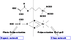
A two-component sol-gel with methacryloyloxy propyltrimethoxysilane and zirconium(IV)-n-propoxide. The top component has an acrylate group that forms an organic network by photopolymerization.
On the (right) side is an inorganic or glass network built around silicon bonded to methoxy groups. In the sol-gel reaction these become OH groups, and Si-O bonds form essentially making glass. The zirconium propoxide is used to adjust the refractive index. By changing the fraction of the organic and inorganic components the refractive index can be adjusted
In waveguides A 95/5 molar ratio of methacryloyloxy propyltrimethoxysilane to zirconium(IV)-n-propoxide is used as a cladding; 85/15 is used for the sol-gel core over a useful range. The solution is hydrolyzed with 0.1 N HCl.
Polymers waveguides can push loss below 0.1 dB/cm
Over the last 25 years loss has improved greatly. This rate of improvement depends on the accumulated knowledge of many workers in the field.
The state of the art waveguide polymer now has loss below .1 dB/cm. We are now competitive with silica on silicon technology but at a much lower cost and is low temperature processable.
Absorption loss
Electronic absorption is neglible for passive materials. In electro-optic materials this kind of loss is significant. Electronic absorption – given by Urbach tail is usually neglible in the near infrared for passive materials.
- <math>\alpha(\omega) = A exp[\sigma (\hbar \omega – \hbar \omega_0) / kT ]\,\!</math>
Vibrational absorption
A fundamental vibration such as carbon – hydrogen is not a problem however the higher harmonics of this vibrations leads to absorption.
Molecular vibrations essentially are high n states of an anharmonic oscillator. This is the dominant source of absorption loss in the near IR .
- <math>E_0 \Rightarrow \sqrt \frac {k} {mu}\,\!</math>
- <math>\mu = \frac {m_c m_x} {m_c + m_x}\,\!</math>
The energy of vibration of a spring like systems is proportional to the square root of the spring constant divided by μ the effective mass of the spring. If mx is hydrogen and mc is carbon then the carbons cancel out and the hydrogen becomes the dominant player.
Using halogen to substitute for hydrogen makes μ larger and therefore makes E0 smaller.
Recall Beer’s law:
- <math>P_{out}= P_{in}e^{-\alpha L}\,\!</math>
Reducing Absorption in polymers
One strategy to improve the absorption is to substitute hydrogen for a heavier version of hydrogen in order to decrease the vibrational energy. The graph shows that by replacing hydrogen with deuterium (upper graph), which is double the mass, does improve the performance at 1310 but this works against you 1350nm. By replacing H with a halogen you can get losses down to .005 dB/cm
See Eldada 1998 [1]
Key Strategies
- Most polymers absorb in near IR (1300 nm- 1600 nm)
- C-H and OH groups have overtones
- Replace hydrogen with fluorine to reduce overtones
To measure absorption you must have a large quantity of the polymer sample. A very pure polished 4.5 cm plug is prepared, measured with a spectrophotometer and absorbance is expressed as an absorption coefficient. This high quality sample of PMMA shows two vibrational peaks.
To convert absorption coefficient (α 1/cm) into decibals:
Loss (dB/cm) = :<math>4.34 \alpha\,\!</math>
See Norwood 1991 [2]
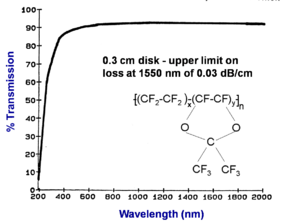
Transmission spectrum of Teflon® AF
A thinner sample of fluorinated polymer (Teflon® AF) containing no hydrogen has very low loss across the entire spectrum from 800nm to 2000 nm. This establishes the upper limit on loss at 1550 nm of 0.03 dB/cm. In this case a .3 cm sample was used and this makes the measurement less reliable than if a thicker sample had been used. This is 10-20 times less loss than PMMA value.
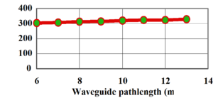
This shows the intensity of light (transmission) passing through an optical waveguide containing a standard sol-gel (containing hydrogen) as a function of pathlength. This shows a loss of 0.8 dB/cm.
A partially fluorinated sol-gel shows higher transmission and a loss of 0.8 dB/cm. The greatest gains can be had by substituting all the hydrogen with halogens.
Polymer Manufacturing into Devices
Polymer waveguide fab: RIE
Reactive Ion Etching (RIE) is used to convert a slab waveguide into a channel waveguide.
- First a slab is prepared with a core layer (higher index of refraction) is placed on a polymer undercladding on a silicon substrate.
- A metallic photo mask is applied to protect the core material.
- A plasma of oxygen is used to eat away the unmasked portion of the polymer.
- The metalic mask is removed and the ribbon of core material is fully encased with overcladding.
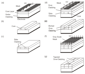
Sol-gel waveguide fabrication
This technique builds a complex sol-gel waveguide using completely wet techniques (no vacuum required). Direct illumination by UV through a mask is able to fix portions of the core in place, while unfixed portions are washed away. A series of steps like this can be used to build a complex device.
Polymer waveguide fab: Results
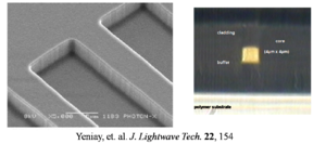
The company Photon X has commercialized the polymer waveguide process. The SEM (5micron line shown) shows very smooth sidewalls from a high quality etching process. Walls can only have roughness of 40-50 nm before there is significant optical loss. The polymer waveguide shows excellent light transmission through a 4 mum x 4 mum waveguide core that has been designed to couple very well with an optical fiber.
See Yeniay [3]
Polymer waveguide fab UV curing
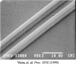
This waveguide is created using the same UV curing process that is used with sol-gels. This shows two waveguides very close to each other. The channel is very difficult to control using photo etching process. The SEM shows a little cross striation but overall very good quality results.
See Viens 1999 [4]
Polymer athermal Array Waveguide Gradiant AWG filter
An array waveguide gradiant is used to separate out wavelengths into separate ports. An athermal device performs equally well at different temperatures without temperature control. To characterize the device you shine a variety of wavelengths through the device simulating various information carriers. The fluorinated polymer device was able to achieve these results:
- Insertion loss: 3 dB
- Adjacent crosstalk: -30dB
- Non-adjacent crosstalk: -28 dB
This passive polymer technology is being used to connect servers (interconnects) in server forms over very short distances with tremendous data rates.
| Previous Topic | Return to Organic Photonics Applications Menu | Next Topic |

