Difference between revisions of "Photoconducting Tip Atomic Force Microscopy pcAFM"
Cmditradmin (talk | contribs) m |
Cmditradmin (talk | contribs) m |
||
| Line 1: | Line 1: | ||
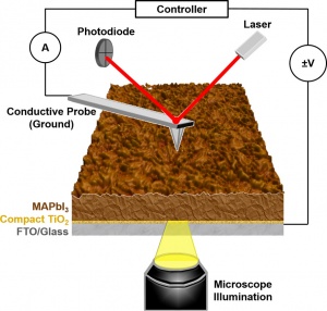
[[ | [[File:PcAFM.jpeg|thumb]]Halide perovskite solar cells based on MAPbI3 and related materials have emerged as the most exciting development in the next generation photovoltaic technologies. Macroscopic characterization techniques usually investigate the performances of these solar cells at the device level with effects of local heterogeneity averaged out, while the photoconductive atomic force microscopy (pcAFM) is able to interrogate the local photovoltaic properties that can be directly traced to their microstructures, shedding light into the microstructural mechanisms that are responsible for the macroscopic performance. | ||
The pcAFM technique is based on the well-known conductive AFM [1], which is capable mapping local current distribution with sensitivity as high as picoampere. When such experiments are carried out under light illumination, pcAFM is realized, as shown in the left figure [2]. It can not only be used to map the local photocurrent characteristics with microstructural features such as grains and grain boundaries (see the simulated 3D topography and pcAFM map below), but also obtain IV curves locally at the nanometer scale by sweeping DC voltage bias while measuring current, thereby extracting short-circuit photocurrent, open-circuit photovoltage, and fill factor. | The pcAFM technique is based on the well-known conductive AFM [1], which is capable mapping local current distribution with sensitivity as high as picoampere. When such experiments are carried out under light illumination, pcAFM is realized, as shown in the left figure [2]. It can not only be used to map the local photocurrent characteristics with microstructural features such as grains and grain boundaries (see the simulated 3D topography and pcAFM map below), but also obtain IV curves locally at the nanometer scale by sweeping DC voltage bias while measuring current, thereby extracting short-circuit photocurrent, open-circuit photovoltage, and fill factor. | ||
A detailed example of pcAFM mapping of MAPbI3 is shown in Fig. 1 of the gallery, and regions of higher and lower photocurrent magnitudes are observed, reflecting structural heterogeneity of the material. Furthermore, with increased DC biases, the photocurrent gradually drops to zero, as expected, and by averaging over higher and lower current regions or the whole area scanned, representative IV curves can be obtained (Fig. 1(b)), from which the open-circuit photovoltage and short-circuit photocurrent density can be estimated in good agreement with macroscopic measurement. | A detailed example of pcAFM mapping of MAPbI3 is shown in Fig. 1 of the gallery, and regions of higher and lower photocurrent magnitudes are observed, reflecting structural heterogeneity of the material. Furthermore, with increased DC biases, the photocurrent gradually drops to zero, as expected, and by averaging over higher and lower current regions or the whole area scanned, representative IV curves can be obtained (Fig. 1(b)), from which the open-circuit photovoltage and short-circuit photocurrent density can be estimated in good agreement with macroscopic measurement. | ||
[[https://byhuang.shinyapps.io/shinyapp/ Complete article ]] | [[https://byhuang.shinyapps.io/shinyapp/ Complete article ]] | ||
Revision as of 15:00, 1 February 2019
Halide perovskite solar cells based on MAPbI3 and related materials have emerged as the most exciting development in the next generation photovoltaic technologies. Macroscopic characterization techniques usually investigate the performances of these solar cells at the device level with effects of local heterogeneity averaged out, while the photoconductive atomic force microscopy (pcAFM) is able to interrogate the local photovoltaic properties that can be directly traced to their microstructures, shedding light into the microstructural mechanisms that are responsible for the macroscopic performance.
The pcAFM technique is based on the well-known conductive AFM [1], which is capable mapping local current distribution with sensitivity as high as picoampere. When such experiments are carried out under light illumination, pcAFM is realized, as shown in the left figure [2]. It can not only be used to map the local photocurrent characteristics with microstructural features such as grains and grain boundaries (see the simulated 3D topography and pcAFM map below), but also obtain IV curves locally at the nanometer scale by sweeping DC voltage bias while measuring current, thereby extracting short-circuit photocurrent, open-circuit photovoltage, and fill factor. A detailed example of pcAFM mapping of MAPbI3 is shown in Fig. 1 of the gallery, and regions of higher and lower photocurrent magnitudes are observed, reflecting structural heterogeneity of the material. Furthermore, with increased DC biases, the photocurrent gradually drops to zero, as expected, and by averaging over higher and lower current regions or the whole area scanned, representative IV curves can be obtained (Fig. 1(b)), from which the open-circuit photovoltage and short-circuit photocurrent density can be estimated in good agreement with macroscopic measurement.
