Difference between revisions of "OFET fabrication and characterization"
Jump to navigation
Jump to search
Cmditradmin (talk | contribs) m (→Significance) |
|||
| Line 13: | Line 13: | ||
===Operation=== | ===Operation=== | ||
{{#ev:youtube|PE8Att1iiFA}} | |||
===Links=== | ===Links=== | ||
see [[Organic_Field_Effect_Transistors]] | see [[Organic_Field_Effect_Transistors]] | ||
Revision as of 13:12, 11 July 2011
Background
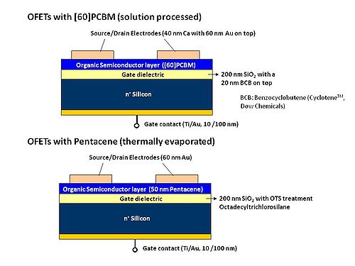
The organic field effect transistor has a layered construction. A voltage applied to the gate causes the polymer layer to become a semiconductor and allows current flow between the source and drain contact.
Significance
<swf width=500 height=400>images/0/04/Ofet_roll_short.swf</swf>
All parts of an OFET can be made from plastics or thin flexible metals so that this could be used for flexible or printed electronics.

