Difference between revisions of "E-beam Lithography"
Jump to navigation
Jump to search
Cmditradmin (talk | contribs) m (New page: E-beam lithography is the process of directing an electron beam across a resist layer and thereby creating a pattern that can be etched. Structures of 20nm can be produced. This is the tec...) |
Cmditradmin (talk | contribs) m |
||
| Line 1: | Line 1: | ||
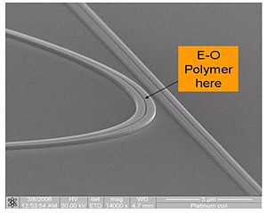
E-beam lithography is the process of directing an electron beam across a resist layer and thereby creating a pattern that can be etched. Structures of 20nm can be produced. This is the technique that is often used to create nano scale waveguides and microring resonators. | E-beam lithography is the process of directing an electron beam across a resist layer and thereby creating a pattern that can be etched. Structures of 20nm can be produced. This is the technique that is often used to create nano scale waveguides and microring resonators. | ||
[[Image:Si waveguide em.jpg|thumb|300px|Silicon waveguide in which EO polymers can be included]] | |||
See Wikipedia [http://en.wikipedia.org/wiki/Electron_beam_lithography E-beam lithography] | See Wikipedia [http://en.wikipedia.org/wiki/Electron_beam_lithography E-beam lithography] | ||
Revision as of 12:06, 10 September 2009
E-beam lithography is the process of directing an electron beam across a resist layer and thereby creating a pattern that can be etched. Structures of 20nm can be produced. This is the technique that is often used to create nano scale waveguides and microring resonators.
See Wikipedia E-beam lithography
