Difference between revisions of "Current OPV Research Directions"
Cmditradmin (talk | contribs) |
Cmditradmin (talk | contribs) |
||
| Line 112: | Line 112: | ||
== Fabrication Processes == | == Fabrication Processes == | ||
[[Image:Nanoimprinting.jpg|thumb|300px|]] | |||
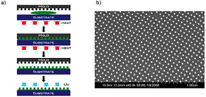
There are real advantages to processing methods which could easily, reproducibly and systematically nano-texture the first-deposited donor or acceptor polymer layer in an organic solar cell (OSC), forming “nano-posts” or “nano-indentations” with optimal lengths and widths, ready for addition of the second component in a bulk heterojunction (BHJ) OSC. As the aspect ratio of such a nanostructure increases, at least an order of magnitude increase in the interfacial area between the donor and acceptor phases is anticipated, thereby greatly enhancing exciton dissociation with retention of vectoral charge transport pathways. Such a processing technique, if scaled to realistic device levels, would remove one of the key limitations to BHJ formation from conventional polymeric materials. Nanoimprint lithography (NIL) involves the formation of nano-posts or nanoindentations in a reusable master stamp, which is then used to emboss a freshly deposited polymer or sol-gel oxide film. This is a process recently developed for creation of grating-like features on optical fibers and waveguides, and is now being scaled to dimensions relevant for OSC device processing. | |||
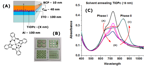
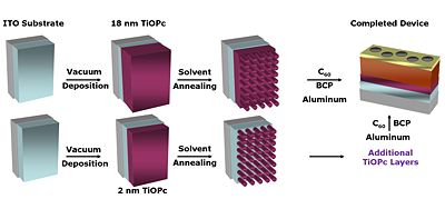
There are new strategies for producing titanyl phthalocyanine (TiOPc) and C60 heterojunctions. After deposition the material can be solvent annealed resulting in nanotexturing and tunability in the NIR. | There are new strategies for producing titanyl phthalocyanine (TiOPc) and C60 heterojunctions. After deposition the material can be solvent annealed resulting in nanotexturing and tunability in the NIR. | ||
[[Image:Solvent_annealing.png|thumb|500px|TiOPc]] | [[Image:Solvent_annealing.png|thumb|500px|TiOPc]] | ||
[[Image:Solvent_annealing_protocols.jpg|thumb|400px|]] | [[Image:Solvent_annealing_protocols.jpg|thumb|400px|a) Nanoimprinting process developed for organic semiconductors; b) SEM picture of nanoimprinted polycarbonate pillars 30 nm wide, 60 nm high and separated by 160 nm (center-to-center) Norwood and Peyghambarian Groups]] | ||
See Armstrong <ref>N. R. Armstrong et al., Adv. Funct. Mater. ; DOI: 10.1002/adfm.200801723</ref> | See Armstrong <ref>N. R. Armstrong et al., Adv. Funct. Mater. ; DOI: 10.1002/adfm.200801723</ref> | ||
Revision as of 13:28, 10 September 2009
| Previous Topic | Return to OPV Menu |
These are promising directions in organic photovoltaic research being pursued at the CMDITR
Evolution of Solar Cell Efficiency
These are the types of efficiencies that people have been able to reach. For example, with silicon, fill factors of about 0.8 and conversion efficiency, of 24% can be reached.
The Grätzel cell, which is a hybrid cell that has both organic and inorganic components and uses a liquid electronlyge, has a conversion efficiency of about 11%. Michael Grätzel is a professor at the technical school of Lausanne in Switzerland.
With polymers, Allen Heeger has recently reported a conversion efficiency of up to 6%. Our goal at this time is to reach the 10% efficiency in organic cells. However, it does not seem to be very easy to achieve.
| Characteristic | Silicon | Organic (Tang) | Organic (Forrest) | Organic (Graetzel) | Polymer | Hybrid nanorods |
|---|---|---|---|---|---|---|
| Open circuit voltage (Voc; V) | 0.7 | 0.45 | 1.02 | 0.721 | 0.63 | 0.7 |
| Short circuit current density (Jsc; mA/cm2) | 43 | 2.3 | 9.7 | 20.53 | 9.5 | 5.7 |
| Voc x Jsc (mW/cm2) | 30.1 | 1.035 | 9.894 | 14.80213 | 5.985 | 3.99 |
| Fill factor (FF) | 0.8 | 0.65 | 0.59 | 0.704 | 0.68 | 0.4 |
| Illumination intensity (mW/cm2) | 100 | 75 | 100 | 100 | 80 | 96.4 |
| Conversion efficiency (%) | 24.08 | 0.9 | 5.7 | 10.4 | 5.1 | 1.7 |
New materials
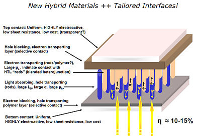
Research directions include using multilayers of small molecules, building polymer blends with interpenetrated networks, nanostructured oxide polymers and hybird approaches using doped inorganics in an organic matrix.
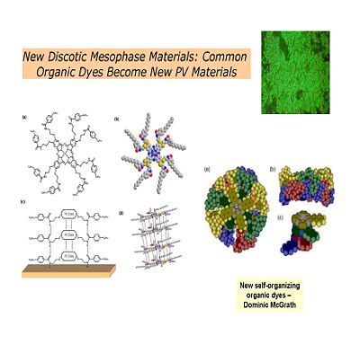
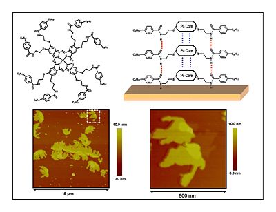
Discotic Mesophase Materials
Dendritic Polymers
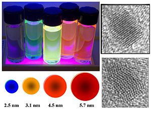
Nanoparticles
Tailored interfaces
Fabrication Processes
There are real advantages to processing methods which could easily, reproducibly and systematically nano-texture the first-deposited donor or acceptor polymer layer in an organic solar cell (OSC), forming “nano-posts” or “nano-indentations” with optimal lengths and widths, ready for addition of the second component in a bulk heterojunction (BHJ) OSC. As the aspect ratio of such a nanostructure increases, at least an order of magnitude increase in the interfacial area between the donor and acceptor phases is anticipated, thereby greatly enhancing exciton dissociation with retention of vectoral charge transport pathways. Such a processing technique, if scaled to realistic device levels, would remove one of the key limitations to BHJ formation from conventional polymeric materials. Nanoimprint lithography (NIL) involves the formation of nano-posts or nanoindentations in a reusable master stamp, which is then used to emboss a freshly deposited polymer or sol-gel oxide film. This is a process recently developed for creation of grating-like features on optical fibers and waveguides, and is now being scaled to dimensions relevant for OSC device processing.
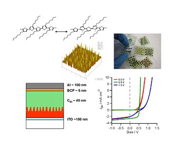
There are new strategies for producing titanyl phthalocyanine (TiOPc) and C60 heterojunctions. After deposition the material can be solvent annealed resulting in nanotexturing and tunability in the NIR.
See Armstrong [1]
References
- ↑ N. R. Armstrong et al., Adv. Funct. Mater. ; DOI: 10.1002/adfm.200801723
| Previous Topic | Return to OPV Menu |
