Difference between revisions of "2D Materials"
Jump to navigation
Jump to search
Cmditradmin (talk | contribs) m |
Cmditradmin (talk | contribs) m |
||
| (2 intermediate revisions by the same user not shown) | |||
| Line 6: | Line 6: | ||
[[File:2d1.png| | [[File:2d1.png|800px]] | ||
[[File:2d2.png| | [[File:2d2.png|800px]] | ||
[[File:2d3.png| | [[File:2d3.png|800px]] | ||
[[File:2d4.png| | [[File:2d4.png|800px]] | ||
Latest revision as of 18:16, 5 February 2019
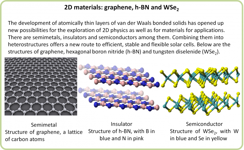
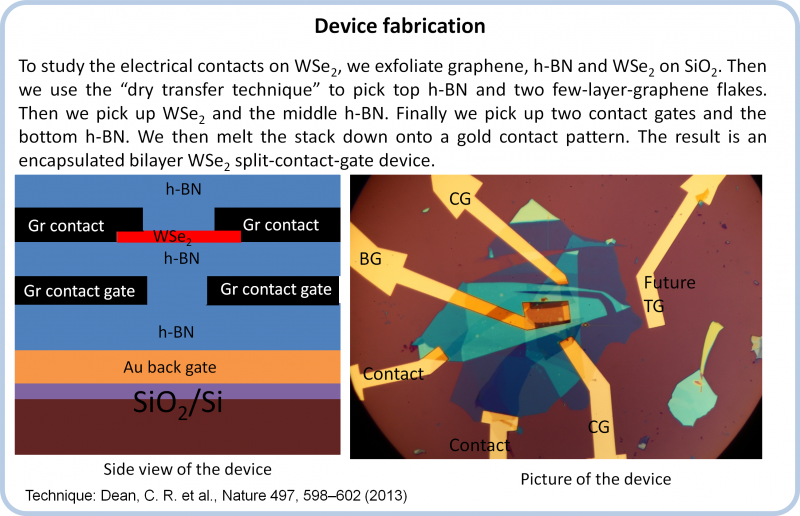
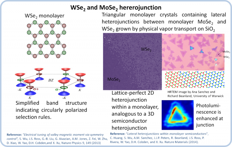
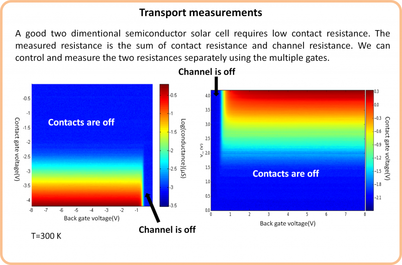
The development of atomically thin layers of van der Waals bonded solids has opened up new possibilities for the exploration of 2D physics as well as for materials for applications. There are semimetals, insulators and semiconductors among them. Combining them into heterostructures offers a new route to efficient, stable and flexible solar cells. Electrical contacts to two dimensional semiconductors-
From poster by Wenjin Zhao, Tauno Palomaki, Joe Finney, Zaiyao Fei, Paul Nguyen, Frank McKay, David H. Cobden Nanodevice Physics Lab, Department of Physics, University of Washington, Seattle WA 98195-1560


