Difference between revisions of "OFET fabrication and characterization"
Jump to navigation
Jump to search
Cmditradmin (talk | contribs) m (→Significance) |
Cmditradmin (talk | contribs) m |
||
| (7 intermediate revisions by 2 users not shown) | |||
| Line 1: | Line 1: | ||
<table id="toc" style="width: 100%"> | |||
<tr> | |||
<td style="text-align: center; width: 33%">[[Main_Page#Synthesis_and_Fabrication|Return to Research Tool Menu]]</td> | |||
</tr> | |||
</table> | |||
===Background=== | ===Background=== | ||
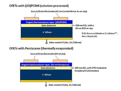
The organic field effect transistor has a layered construction. A voltage applied to the gate causes the polymer layer to become a semiconductor and allows current flow between the source and drain contact. | The organic field effect transistor has a layered construction. A voltage applied to the gate causes the polymer layer to become a semiconductor and allows current flow between the source and drain contact. | ||
===Significance=== | ===Significance=== | ||
<swf width=500 height=400>images/0/04/Ofet_roll_short.swf</swf> | |||
All parts of an OFET can be made from plastics or thin flexible metals so that this could be used for flexible or printed electronics. | All parts of an OFET can be made from plastics or thin flexible metals so that this could be used for flexible or printed electronics. | ||
[[Image:OFET-2Device_structures.jpg|thumb| | |||
[[Image:OFET-2Device_structures.jpg|thumb|left|500px|Solution processed and thermally evaporated OFET Device structures]] | |||
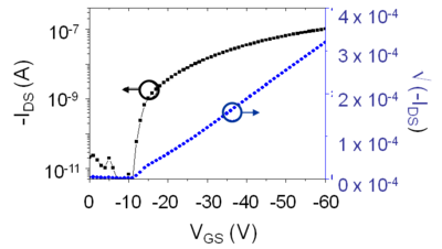
[[Image:Transfer_curve.png|thumb|400px|right| The OFET transfer curve showing source drain current in black and the squareroot of the source drain current in blue, plotted against the gate voltage. ]] | |||
<br clear='all'> | |||
===Operation=== | ===Operation=== | ||
{{#ev:youtube|PE8Att1iiFA}} | |||
===Links=== | ===Links=== | ||
see [[Organic_Field_Effect_Transistors]] | |||
Latest revision as of 10:43, 11 October 2011
| Return to Research Tool Menu |
Background
The organic field effect transistor has a layered construction. A voltage applied to the gate causes the polymer layer to become a semiconductor and allows current flow between the source and drain contact.
Significance
<swf width=500 height=400>images/0/04/Ofet_roll_short.swf</swf>
All parts of an OFET can be made from plastics or thin flexible metals so that this could be used for flexible or printed electronics.

