Difference between revisions of "E-beam Lithography"
Cmditradmin (talk | contribs) m |
Cmditradmin (talk | contribs) m (moved E-beam lithographys to E-beam Lithography) |
||
| (14 intermediate revisions by 2 users not shown) | |||
| Line 1: | Line 1: | ||
E-beam lithography is the process of directing an electron beam across a resist layer and thereby creating a pattern that can be etched. Structures of 20nm can be produced. This is the technique that is often used to create nano scale waveguides and microring resonators. | <table id="toc" style="width: 100%"> | ||
<tr> | |||
<td style="text-align: center; width: 33%">[[Main_Page#Synthesis_and_Fabrication|Return to Research Tool Menu]]</td> | |||
</tr> | |||
</table> | |||
=== Overview === | |||
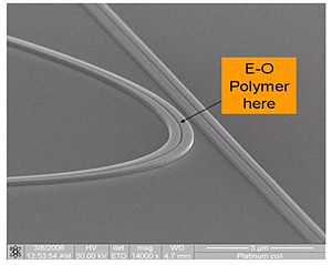
E-beam lithography is the process of directing an electron beam across a resist layer and thereby creating a pattern that can be etched. Structures of 20nm can be produced. This is the technique that is often used to create nano scale waveguides and microring resonators. One type uses an scanning electron microscope equipped with special beam control software. The other far more expensive method is a dedicated e-beam facility that is able to etch structures directly. | |||
[[Image:Si waveguide em.jpg|thumb|300px|Silicon waveguide in which EO polymers can be included]] | [[Image:Si waveguide em.jpg|thumb|300px|Silicon waveguide in which EO polymers can be included]] | ||
The Scanning Electron Microscope can be used to expose light sensitive resist allowing the production of extremely fine detail features by etching. This is convenient for doing single prototypes but is since the process is relatively slow it is not practical for multiple manufacturing runs. | |||
=== SEM with Nabity === | |||
The Nabity Nanometer Pattern Generation System (NPGS) combined with the Sirion SEM provides a user-friendly tool for the fabrication of nanostructures as small as 20 nm on a variety of materials including PMMA, SU8, and copolymers (MMA (8.5) and MMA EL 11). There are three basic steps involved in the generation of nano- or micro-scale patterns: (1) pattern design; (2) creation of a NPGS run file; and (3) pattern writing with alignment for multilayer lithography. | |||
#Patterns are created using DesignCAD and they may also be imported from DWG, DXF, GDSII, CIF, and IGES file formats. | |||
#An NPGS "run file" includes the exposure conditions for the different drawing elements in the pattern. Advanced features include global stage corrections, pattern arrays, x-y-focus, external commands, and fracturing of large patterns. | |||
#The NPGS identifies the writing (PG) and alignment (AL) programs in a "run file". PG writes a pattern by simultaneously controlling the x-y scan coils and beam blanking of the microscope. AL allows the alignment of patterns to existing alignment marks without exposing the writing area. | |||
<swf width="500" height="400">images/b/bd/Ebeamlith.swf</swf> | |||
=== Operation === | |||
Part 1: | |||
{{#ev:youtube|bvgITKqYpuY}} | |||
Part 2: | |||
{{#ev:youtube|fZmC5xeHHaw}} | |||
Part 3: | |||
{{#ev:youtube|ktkDqofYfMY}} | |||
=== External Links === | |||
*[http://www.jcnabity.com/ JC Nabity website for SEM e-beam conversion] | |||
*[[wikipedia:Electron_beam_lithography E-beam lithography]] | |||
*[http://www.microscopy-analysis.com/news/university-washington-orders-jeol-jbx-6300fs-direct-write-e-beam-lithography-system-microfabric UW Jeol E-beam] | |||
Latest revision as of 08:42, 18 October 2011
| Return to Research Tool Menu |
Overview
E-beam lithography is the process of directing an electron beam across a resist layer and thereby creating a pattern that can be etched. Structures of 20nm can be produced. This is the technique that is often used to create nano scale waveguides and microring resonators. One type uses an scanning electron microscope equipped with special beam control software. The other far more expensive method is a dedicated e-beam facility that is able to etch structures directly.
The Scanning Electron Microscope can be used to expose light sensitive resist allowing the production of extremely fine detail features by etching. This is convenient for doing single prototypes but is since the process is relatively slow it is not practical for multiple manufacturing runs.
SEM with Nabity
The Nabity Nanometer Pattern Generation System (NPGS) combined with the Sirion SEM provides a user-friendly tool for the fabrication of nanostructures as small as 20 nm on a variety of materials including PMMA, SU8, and copolymers (MMA (8.5) and MMA EL 11). There are three basic steps involved in the generation of nano- or micro-scale patterns: (1) pattern design; (2) creation of a NPGS run file; and (3) pattern writing with alignment for multilayer lithography.
- Patterns are created using DesignCAD and they may also be imported from DWG, DXF, GDSII, CIF, and IGES file formats.
- An NPGS "run file" includes the exposure conditions for the different drawing elements in the pattern. Advanced features include global stage corrections, pattern arrays, x-y-focus, external commands, and fracturing of large patterns.
- The NPGS identifies the writing (PG) and alignment (AL) programs in a "run file". PG writes a pattern by simultaneously controlling the x-y scan coils and beam blanking of the microscope. AL allows the alignment of patterns to existing alignment marks without exposing the writing area.
<swf width="500" height="400">images/b/bd/Ebeamlith.swf</swf>
Operation
Part 1:
Part 2:
Part 3:
