Difference between revisions of "The Need for Photonic Integration"
Cmditradmin (talk | contribs) m |
|||
| (19 intermediate revisions by 2 users not shown) | |||
| Line 1: | Line 1: | ||
<table id="toc" style="width: 100%"> | |||
<tr> | |||
<td style="text-align: center; width: 33%">[[Main_Page#Photonics Integration|Photonics Integration Menu]]</td> | |||
<td style="text-align: right; width: 33%">[[Photonics Integration|Next Topic]]</td> | |||
</tr> | |||
</table> | |||
This wiki is largely drawn from a presentation by Larry Dalton delivered July 21, 2008. The steaming version of the persentation is available [http://lectures.stc-mditr.org/tegrity/smhunter/gradmodules_2A/larry%20dalton63088490-410b-4ca3-a84ee9e9e-19f8-44be-b265-1b688070529d/Class/TegrityPlayer.htm? here]. | This wiki is largely drawn from a presentation by Larry Dalton delivered July 21, 2008. The steaming version of the persentation is available [http://lectures.stc-mditr.org/tegrity/smhunter/gradmodules_2A/larry%20dalton63088490-410b-4ca3-a84ee9e9e-19f8-44be-b265-1b688070529d/Class/TegrityPlayer.htm? here]. | ||
One of the things that we all face as | One of the things that we all face as scientists is deciding what topics we want to pursue for our research career. Two things are useful. One is the professional society which hold special symposia on hot topics such as high temperature super conductivity. An ever better avenue is the workshops that funding agencies hold on emerging topics. In 2007 both the NSF and the Defense Science Board, which make recommendations for defense spending, held workshops on photonics integration. So this is perceived as a hot research topic. | ||
| Line 9: | Line 18: | ||
=== Trends for Data in Telecommunications === | === Trends for Data in Telecommunications === | ||
[[Image:800px-Heliograph.jpg|thumb|300px|Signaling with Mance heliograph, 1910]] | [[Image:800px-Heliograph.jpg|thumb|300px|Signaling with Mance heliograph, 1910]] | ||
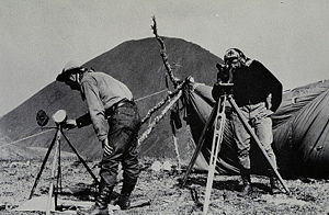
The history of modern telecommunication by wire and wireless dates back to the telephone | The history of modern telecommunication by wire and wireless dates back to the telephone, which transduces the phonon vibrations of the human voice into electrical signals that are carried over copper wire. Wireless telecommunication date back to the heliograph, which uses mechancial modulation of light. These original devices had very limited bandwidth because a shutter can only run so fast. Copper wire was ok for the amount of data that a voice stream demands. Telecommunications has evolved to support "machine-to-machine" telecommunications. This has placed dramatically larger demands on bandwidth– the amount of information sent per unit time. We also want more capability in smaller and smaller devices. Copper has given away to optical fiber. Wireless frequencies has extended to 100 gigahertz carriers, eg gGigabeam inc. You only have to look at the advertisements for bandwidth and integration for consumer devices to release how important these have become as drivers. | ||
=== Moore’s Law- the History of Integration === | === Moore’s Law- the History of Integration === | ||
[[Image:Mooreslaw.jpg|thumb|400px|The size of features has been decreasing.]] | [[Image:Mooreslaw.jpg|thumb|400px|The size of features has been decreasing.]] | ||
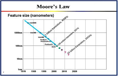
Nano-engineering has been around for a long time. For example silicon CMOS technology has built smaller and smaller transistors and placed more transistors on a chip. Moore’s law shows feature size decreasing over the years and has allowed us to place 10 billion transistors on a chip in 2010 with a bandwidth of 30 GHz. This has resulted in a great reduction in cost. You can buy a computer today for about the same cost as 30 years ago but the functionality has exponentially increased. Tools such as reactive ion etching (RIE) and e-beam lithography have enabled nano-engineering. | Nano-engineering has been around for a long time. For example, silicon CMOS technology has built smaller and smaller transistors and placed more transistors on a chip. Moore’s law shows feature size decreasing over the years and has allowed us to place 10 billion transistors on a chip in 2010 with a bandwidth of 30 GHz. This has resulted in a great reduction in cost. You can buy a computer today for about the same cost as 30 years ago but the functionality has exponentially increased. Tools such as reactive ion etching (RIE) and [[e-beam lithography]] have enabled nano-engineering. | ||
[[Image:700px-Moore_Law_diagram_(2004).png|frame|400px|The number of transistors on a chip are steadily increasing.]] | [[Image:700px-Moore_Law_diagram_(2004).png|frame|400px|The number of transistors on a chip are steadily increasing.]] | ||
| Line 22: | Line 31: | ||
We take for granted the dramatic impact that these changes have had on how we live. Information technology is one of the three largest component (energy and agriculture are the other two ) and is the fastest growing component of the world economy. One third to one half of the world’s population will be employed in information technology by the year 2010. It will have a greater impact in the next 20 years because of electronic/photonic integration and nano-engineered materials. | We take for granted the dramatic impact that these changes have had on how we live. Information technology is one of the three largest component (energy and agriculture are the other two ) and is the fastest growing component of the world economy. One third to one half of the world’s population will be employed in information technology by the year 2010. It will have a greater impact in the next 20 years because of electronic/photonic integration and nano-engineered materials. | ||
Moore’s law talks specifically about electronic device integration. But photonics play a major role about everything we know about the universe, for example your eyes are photodetectors. | Moore’s law talks specifically about electronic device integration. But photonics play a major role about everything we know about the universe, for example your eyes are photodetectors. There is now both top-down nano-engineering with electronic integration but also “bottom up engineering”– starting with molecules and building up to structures. | ||
<br clear='all'> | <br clear='all'> | ||
| Line 28: | Line 37: | ||
=== Phototonic information / energy processing === | === Phototonic information / energy processing === | ||
[[Image:photon_uses.JPG|thumb| | [[Image:photon_uses.JPG|thumb|400px|Photonics applications]] | ||
Photons are important. They can be used to; | Photons are important. They can be used to; | ||
| Line 36: | Line 45: | ||
*Energize- light energy can be changed into electrical energy in solar cells. | *Energize- light energy can be changed into electrical energy in solar cells. | ||
*Actuate- high power laser light can be used to weld and cut, or perform delicate medical procedures | *Actuate- high power laser light can be used to weld and cut, or perform delicate medical procedures | ||
*Transport-Information over the telephone is carried by photons on optical fiber. | *Transport- Information over the telephone is carried by photons on optical fiber. | ||
*Store- optical memories such as CDs and DVD are created and read by photons. | *Store- optical memories such as CDs and DVD are created and read by photons. | ||
<br clear='all'> | <br clear='all'> | ||
[[Image:Sensing_imaging.JPG|thumb|300px|New sensing technology creates a flood of data.]] | [[Image:Sensing_imaging.JPG|thumb|300px|New sensing technology creates a flood of data.]] | ||
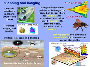
Sensor technology has been evolving at a collosal rate so we have deal with more and more data. Now we use sensor paints that let us monitor pressure. An airplane in a wind tunnel is covered with pressure sensitive paint and reveals using color the instantaneous pressure on the surface. Biocompatible paints could be applied to a honeybees wing to study its performance during flight. Nanophotonics sensors can be combined with microfluidics allow for point of care diagnostic chips, for real time diagnosis of any chemical. Collision avoidance radar can be integrated with automatic cruise control on vehicles. Terahertz imaging can see inside normally opaque materials with low energy radiation. All this leads to flood of information. | New sources of data. | ||
Sensor technology has been evolving at a collosal rate so we have deal with more and more data. Now we can use sensor paints that let us monitor pressure. An airplane in a wind tunnel is covered with pressure sensitive paint and reveals using color the instantaneous pressure on the surface. Biocompatible paints could be applied to a honeybees wing to study its performance during flight. Nanophotonics sensors can be combined with microfluidics allow for point-of-care diagnostic chips, for real time diagnosis of any chemical. Collision avoidance radar can be integrated with automatic cruise control on vehicles. Terahertz imaging can see inside normally opaque materials with low energy radiation. All this leads to flood of information. | |||
<br clear='all'> | <br clear='all'> | ||
=== Particles suitable for telecommunication === | === Particles suitable for telecommunication === | ||
In the universe there four types of particles involved in the communication of information. | In the universe there are four types of particles involved in the communication of information. | ||
'''Electrons'''—Negatively charged particles and the lightest of the three particles (electrons, protons, and neutrons) that make up atoms. The electron is most easily perturbed by the application of an electric field. If you take an single atom the energy levels are quantized. The highest occupied orbital is bound state so electrons are localized. But in metals, electrons in the highest occupied band conists of electrons that are not tightly bound to any specific atom known as the conduction band. That movement can be used convey information. | '''Electrons'''—Negatively charged particles and the lightest of the three particles (electrons, protons, and neutrons) that make up atoms. The electron is most easily perturbed by the application of an electric field. If you take an single atom the energy levels are quantized. The highest occupied orbital is bound state so electrons are localized. But in metals, electrons in the highest occupied band conists of electrons that are not tightly bound to any specific atom known as the conduction band. That movement can be used to convey information. | ||
'''Photons'''—The smallest (quantized) units of light. | '''Photons'''—The smallest (quantized) units of light. | ||
'''Phonons''' | '''Phonons'''—These are quantized vibrations or quantized sound waves; however these are short ranged so we will ignore them. We have to convert phonons into electrical or optical signals in order to convey them over distance. | ||
'''Plasmons''' | '''Plasmons'''—These are quantized waves in metals excited by light. These are short ranged so we will ignore. They are useful for engineering extremely small scale circuits connected by nanowires carrying plasmons. | ||
=== What is the best information carrier, electrons or photons? === | === What is the best information carrier, electrons or photons? === | ||
[[Image:photonic_decisiongraph.JPG|thumb|400px|]] | [[Image:photonic_decisiongraph.JPG|thumb|400px|]] | ||
Electrons are fermions. They are strongly interacting with matter. | '''Electrons are fermions'''. They are strongly interacting with matter. They can be sent down a copper wire. Conduction electrons are equally well positioned by any metal atom along the wire once we apply an electric field as a driving force to send them in a direction. However they scatter off nuclei and with increased temperature the vibrational energy of nuclei increases so the scattering becomes worse; the resistivity to the electrons moving down a wire increases with temperature. Electrons also interact strongly with each other, so it very difficult to propagate electrons over long distances through metal wire. | ||
'''Photons are bosons'''. They are weakly interacting particles. They have nearly unlimited bandwidth. The transmission through optical fiber has very low loss so we can send signals around the world by fiber. When you want bandwidth and to transport over “large” distances, use photons; when other factors such as computing are important use electrons. | |||
Companies like Intel and IBM use decision graphs to help to determine when to process information using photons as opposed to electrons. The graphs compare optical to electrical performance as a function of time, for a variety of parameter such as cost, power and information density. Starting in 2006 photonics was preferred to send information farther than 10 meters. In 2008 photonics is indicated for all applications except for a cost factor even over short distances. This has led to determined efforts by Intel and IBM to integrate photonic technology directly on electronic chips. | |||
== Drivers for Integration == | == Drivers for Integration == | ||
| Line 70: | Line 81: | ||
Computing – Connecting chip-to-chip and within a chip (chipscale) | Computing – Connecting chip-to-chip and within a chip (chipscale) | ||
'''Telecommunications (photonics already critical)''' | |||
Telecommunications (photonics already critical) | |||
*Fiber | *Fiber | ||
* | *Wireless | ||
Sensing and imaging (photonics already critical) | '''Sensing and imaging (photonics already critical)''' | ||
* | *Point-of-care medical diagnostics which attempts to provide doctors with a simple chip that can used right in the examination room, more reliably and inexpensively compared to sending a sample out to a diagnostic lab. | ||
* | *Spectroscopy (including THz) – we may be able to build chipscale spectrometers | ||
* | *Embedded network sensing- Bridge, gas pipelines and environmental areas will have distributed network sensors that combine combines sensors, microprocessor, telecommunications, even actuators and energy source all on the same chip. | ||
*Entertainment (iPOD, iPhone, Gaming, Cameras, etc.) | *Entertainment (iPOD, iPhone, Gaming, Cameras, etc.) | ||
| Line 90: | Line 97: | ||
SWAP - Engineers worry about SWAP(Size, Weight, and Power). All can be decreased using photonics integration. | SWAP - Engineers worry about SWAP(Size, Weight, and Power). All can be decreased using photonics integration. | ||
Performance | '''Performance''' | ||
*Bandwidth- can be increased | *Bandwidth- can be increased | ||
*Drive voltage- Drive voltage can be decreased. If you go from electrical to optical and back to electrical you can increase the electrical signal (gain). | *Drive voltage- Drive voltage can be decreased. If you go from electrical to optical and back to electrical you can increase the electrical signal (gain). | ||
*Thermal management- high density of transistors creates heat and this has become a serious problem. | |||
*Latency (speed) – You can’t move high amounts of data even short distances without photonics. | |||
Manufacturing yield, in-field reliability and cost | '''Manufacturing yield, in-field reliability and cost''' | ||
*Silicon CMOS is the poster child | *Silicon CMOS is the poster child for manufacturing efficiency. | ||
*Avoid fragile interconnects- All connection are built in to the chip | *Avoid fragile interconnects- All connection are built in to the chip | ||
*Avoid the cost and defects associated with manual labor- The human made solder | *Avoid the cost and defects associated with manual labor- The human-made solder joints are the most common defect. Automation decreases cost and increases reliability. | ||
*Facilitates rapid and reliable testing- With a single chip you can build an rigorous automated test. (quality control) | *Facilitates rapid and reliable testing- With a single chip you can build an rigorous automated test. (quality control) | ||
== Schema == | |||
[[Image:EPintegration_schema.JPG|thumb|400px|]] | |||
== Two types of Integration == | On the same chip there must be instantaneous, seamless interconversion of electrical and optical signals. This entails two fundamental operations; | ||
*First we would like to take '''electrical information''' from one cell to another cell. To do this we have encode it on an optical signal. | |||
*A second operation is to take an '''optical signal''', for example from an optical sensor, and take the information into an electrical logic cell of a microprocessor. | |||
=== Two types of Integration === | |||
[[Image:EOchip.jpg|thumb|300px|Schematic of electro optical integrated chip]] | [[Image:EOchip.jpg|thumb|300px|Schematic of electro optical integrated chip]] | ||
Integration requires a series of science and technology advances before | Integration requires a series of science and technology advances before a product can be made that people will spend money on, e.g. the MP3 player. Since 2000 all the major journals in EE have been covering photonics integration. Many federal funding agencies are trying to move this vision forward. | ||
'''Type 1''' integration is already here. Type one refers to simply taking the photonic devices such as lasers, modulators and optical circuitry and attaching it by conventional means like wires and fibers to electronic technology. You can replace 10 electrical coaxial cables with one optical fiber. Many of our older military aircraft are being retrofitted to remove electrical wire. This saves weight and size, reduces power consumption, and limits vulnerability to electromagnetic interference. | |||
The same thing is happening in the computer industry. The IBM Federation Switch for ASCI Purple has converted coaxial copper cables (issues: bulk, bend, weight, blockage of air cooling) to optical (issue: cost). | |||
'''Type 2''' is the future. Photonic and electronic function is on the same multi-layer chip. The chip has a processor plane over memory planes, on top of a photonic network interconnect plane that includes optical devices, electronic drivers and amplifiers and electronic control network. | |||
We are envisioning a Smart Card | We are envisioning a Smart Card | ||
| Line 120: | Line 133: | ||
*Digital memoir-PDA | *Digital memoir-PDA | ||
On a larger scale many of these devices are connected to each other through a community optical network. To integrate all the possible components we need to be able to seamlessly convert back and forth between optical and electrical signal domains. | |||
To integrate all the possible components we need to be able to seamlessly convert back and forth between optical and electrical signal domains. | |||
[[category:photonics applications]] | |||
[[category:materials processing and fabrication]] | |||
<table id="toc" style="width: 100%"> | |||
<tr> | |||
<td style="text-align: center; width: 33%">[[Main_Page#Photonics Integration|Photonics Integration Menu]]</td> | |||
<td style="text-align: right; width: 33%">[[Photonics Integration|Next Topic]]</td> | |||
</tr> | |||
</table> | |||
Latest revision as of 13:30, 29 December 2009
| Photonics Integration Menu | Next Topic |
This wiki is largely drawn from a presentation by Larry Dalton delivered July 21, 2008. The steaming version of the persentation is available here.
One of the things that we all face as scientists is deciding what topics we want to pursue for our research career. Two things are useful. One is the professional society which hold special symposia on hot topics such as high temperature super conductivity. An ever better avenue is the workshops that funding agencies hold on emerging topics. In 2007 both the NSF and the Defense Science Board, which make recommendations for defense spending, held workshops on photonics integration. So this is perceived as a hot research topic.
Telecommunications
Trends for Data in Telecommunications
The history of modern telecommunication by wire and wireless dates back to the telephone, which transduces the phonon vibrations of the human voice into electrical signals that are carried over copper wire. Wireless telecommunication date back to the heliograph, which uses mechancial modulation of light. These original devices had very limited bandwidth because a shutter can only run so fast. Copper wire was ok for the amount of data that a voice stream demands. Telecommunications has evolved to support "machine-to-machine" telecommunications. This has placed dramatically larger demands on bandwidth– the amount of information sent per unit time. We also want more capability in smaller and smaller devices. Copper has given away to optical fiber. Wireless frequencies has extended to 100 gigahertz carriers, eg gGigabeam inc. You only have to look at the advertisements for bandwidth and integration for consumer devices to release how important these have become as drivers.
Moore’s Law- the History of Integration
Nano-engineering has been around for a long time. For example, silicon CMOS technology has built smaller and smaller transistors and placed more transistors on a chip. Moore’s law shows feature size decreasing over the years and has allowed us to place 10 billion transistors on a chip in 2010 with a bandwidth of 30 GHz. This has resulted in a great reduction in cost. You can buy a computer today for about the same cost as 30 years ago but the functionality has exponentially increased. Tools such as reactive ion etching (RIE) and e-beam lithography have enabled nano-engineering.
Impact of Information Technology
We take for granted the dramatic impact that these changes have had on how we live. Information technology is one of the three largest component (energy and agriculture are the other two ) and is the fastest growing component of the world economy. One third to one half of the world’s population will be employed in information technology by the year 2010. It will have a greater impact in the next 20 years because of electronic/photonic integration and nano-engineered materials.
Moore’s law talks specifically about electronic device integration. But photonics play a major role about everything we know about the universe, for example your eyes are photodetectors. There is now both top-down nano-engineering with electronic integration but also “bottom up engineering”– starting with molecules and building up to structures.
Photonics
Phototonic information / energy processing
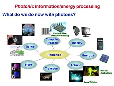
Photons are important. They can be used to;
- Sense- photodetectors are used in cameras and imaging.
- Compute, process- including photonic time domain processing, optical code readers
- Display- The computer display, calculator or digital watch use photons.
- Energize- light energy can be changed into electrical energy in solar cells.
- Actuate- high power laser light can be used to weld and cut, or perform delicate medical procedures
- Transport- Information over the telephone is carried by photons on optical fiber.
- Store- optical memories such as CDs and DVD are created and read by photons.
New sources of data.
Sensor technology has been evolving at a collosal rate so we have deal with more and more data. Now we can use sensor paints that let us monitor pressure. An airplane in a wind tunnel is covered with pressure sensitive paint and reveals using color the instantaneous pressure on the surface. Biocompatible paints could be applied to a honeybees wing to study its performance during flight. Nanophotonics sensors can be combined with microfluidics allow for point-of-care diagnostic chips, for real time diagnosis of any chemical. Collision avoidance radar can be integrated with automatic cruise control on vehicles. Terahertz imaging can see inside normally opaque materials with low energy radiation. All this leads to flood of information.
Particles suitable for telecommunication
In the universe there are four types of particles involved in the communication of information.
Electrons—Negatively charged particles and the lightest of the three particles (electrons, protons, and neutrons) that make up atoms. The electron is most easily perturbed by the application of an electric field. If you take an single atom the energy levels are quantized. The highest occupied orbital is bound state so electrons are localized. But in metals, electrons in the highest occupied band conists of electrons that are not tightly bound to any specific atom known as the conduction band. That movement can be used to convey information.
Photons—The smallest (quantized) units of light.
Phonons—These are quantized vibrations or quantized sound waves; however these are short ranged so we will ignore them. We have to convert phonons into electrical or optical signals in order to convey them over distance.
Plasmons—These are quantized waves in metals excited by light. These are short ranged so we will ignore. They are useful for engineering extremely small scale circuits connected by nanowires carrying plasmons.
What is the best information carrier, electrons or photons?
Electrons are fermions. They are strongly interacting with matter. They can be sent down a copper wire. Conduction electrons are equally well positioned by any metal atom along the wire once we apply an electric field as a driving force to send them in a direction. However they scatter off nuclei and with increased temperature the vibrational energy of nuclei increases so the scattering becomes worse; the resistivity to the electrons moving down a wire increases with temperature. Electrons also interact strongly with each other, so it very difficult to propagate electrons over long distances through metal wire.
Photons are bosons. They are weakly interacting particles. They have nearly unlimited bandwidth. The transmission through optical fiber has very low loss so we can send signals around the world by fiber. When you want bandwidth and to transport over “large” distances, use photons; when other factors such as computing are important use electrons.
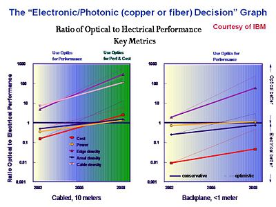
Companies like Intel and IBM use decision graphs to help to determine when to process information using photons as opposed to electrons. The graphs compare optical to electrical performance as a function of time, for a variety of parameter such as cost, power and information density. Starting in 2006 photonics was preferred to send information farther than 10 meters. In 2008 photonics is indicated for all applications except for a cost factor even over short distances. This has led to determined efforts by Intel and IBM to integrate photonic technology directly on electronic chips.
Drivers for Integration
Economic drivers for integration
What are the economic drivers for chipscale electronic/photonic integration? Computing – Connecting chip-to-chip and within a chip (chipscale)
Telecommunications (photonics already critical)
- Fiber
- Wireless
Sensing and imaging (photonics already critical)
- Point-of-care medical diagnostics which attempts to provide doctors with a simple chip that can used right in the examination room, more reliably and inexpensively compared to sending a sample out to a diagnostic lab.
- Spectroscopy (including THz) – we may be able to build chipscale spectrometers
- Embedded network sensing- Bridge, gas pipelines and environmental areas will have distributed network sensors that combine combines sensors, microprocessor, telecommunications, even actuators and energy source all on the same chip.
- Entertainment (iPOD, iPhone, Gaming, Cameras, etc.)
Technology Drivers
What the technology drivers of integration? SWAP - Engineers worry about SWAP(Size, Weight, and Power). All can be decreased using photonics integration.
Performance
- Bandwidth- can be increased
- Drive voltage- Drive voltage can be decreased. If you go from electrical to optical and back to electrical you can increase the electrical signal (gain).
- Thermal management- high density of transistors creates heat and this has become a serious problem.
- Latency (speed) – You can’t move high amounts of data even short distances without photonics.
Manufacturing yield, in-field reliability and cost
- Silicon CMOS is the poster child for manufacturing efficiency.
- Avoid fragile interconnects- All connection are built in to the chip
- Avoid the cost and defects associated with manual labor- The human-made solder joints are the most common defect. Automation decreases cost and increases reliability.
- Facilitates rapid and reliable testing- With a single chip you can build an rigorous automated test. (quality control)
Schema
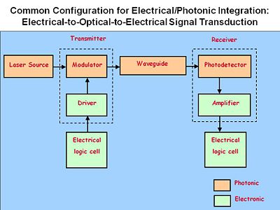
On the same chip there must be instantaneous, seamless interconversion of electrical and optical signals. This entails two fundamental operations;
- First we would like to take electrical information from one cell to another cell. To do this we have encode it on an optical signal.
- A second operation is to take an optical signal, for example from an optical sensor, and take the information into an electrical logic cell of a microprocessor.
Two types of Integration
Integration requires a series of science and technology advances before a product can be made that people will spend money on, e.g. the MP3 player. Since 2000 all the major journals in EE have been covering photonics integration. Many federal funding agencies are trying to move this vision forward.
Type 1 integration is already here. Type one refers to simply taking the photonic devices such as lasers, modulators and optical circuitry and attaching it by conventional means like wires and fibers to electronic technology. You can replace 10 electrical coaxial cables with one optical fiber. Many of our older military aircraft are being retrofitted to remove electrical wire. This saves weight and size, reduces power consumption, and limits vulnerability to electromagnetic interference. The same thing is happening in the computer industry. The IBM Federation Switch for ASCI Purple has converted coaxial copper cables (issues: bulk, bend, weight, blockage of air cooling) to optical (issue: cost).
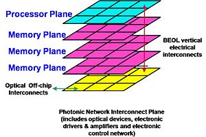
Type 2 is the future. Photonic and electronic function is on the same multi-layer chip. The chip has a processor plane over memory planes, on top of a photonic network interconnect plane that includes optical devices, electronic drivers and amplifiers and electronic control network.
We are envisioning a Smart Card
- Cell Phone/Text messaging
- Camera
- Wallet—financial management center
- EMR Key access to house & car
- Mobile test laboratory-health monitoring
- Computer
- Digital memoir-PDA
On a larger scale many of these devices are connected to each other through a community optical network. To integrate all the possible components we need to be able to seamlessly convert back and forth between optical and electrical signal domains.
| Photonics Integration Menu | Next Topic |
