Difference between revisions of "Current OPV Research Directions"
Cmditradmin (talk | contribs) |
Cmditradmin (talk | contribs) m (→Nanoparticles) |
||
| (44 intermediate revisions by 2 users not shown) | |||
| Line 1: | Line 1: | ||
[[Main_Page#Organic Solar Cells|Return to OPV Menu]] | | <table id="toc" style="width: 100%"> | ||
<tr> | |||
<td style="text-align: left; width: 33%">[[Energy vs Charge Transfer at Heterojunctions|Previous Topic]]</td> | |||
<td style="text-align: center; width: 33%">[[Main_Page#Organic Solar Cells|Return to OPV Menu]]</td> | |||
</tr> | |||
</table> | |||
These are promising directions in organic photovoltaic research being pursued at the CMDITR | |||
== Evolution of Solar Cell Efficiency == | |||
These are the types of efficiencies that people have been able to reach. For example, with silicon, fill factors of about 0.8 and conversion efficiency, of 24% can be reached. | |||
The Grätzel cell, which is a hybrid cell that has both organic and inorganic components and uses a liquid electrolyte, has a conversion efficiency of about 11%. Michael Grätzel is a professor at the technical school of Lausanne in Switzerland. | |||
With polymers, Allen Heeger has recently reported a conversion efficiency of up to 6%. Our goal at this time is to reach the 10% efficiency in organic cells. However, it does not seem to be very easy to achieve. | |||
{| class="wikitable" border = "1" | |||
|- | |||
! Characteristic | |||
! Silicon | |||
! Organic (Tang) | |||
! Organic (Forrest) | |||
! Organic (Graetzel) | |||
! Polymer | |||
! Hybrid nanorods | |||
|- | |||
| Open circuit voltage (Voc; V) | |||
| 0.7 | |||
| 0.45 | |||
|1.02 | |||
|0.721 | |||
|0.63 | |||
|0.7 | |||
|- | |||
|Short circuit current density (Jsc; mA/cm2) | |||
|43 | |||
|2.3 | |||
|9.7 | |||
|20.53 | |||
|9.5 | |||
|5.7 | |||
|- | |||
|Voc x Jsc (mW/cm2) | |||
|30.1 | |||
|1.035 | |||
|9.894 | |||
|14.80213 | |||
|5.985 | |||
|3.99 | |||
|- | |||
|Fill factor (FF) | |||
|0.8 | |||
|0.65 | |||
|0.59 | |||
|0.704 | |||
|0.68 | |||
|0.4 | |||
|- | |||
|Illumination intensity (mW/cm2) | |||
|100 | |||
|75 | |||
|100 | |||
|100 | |||
|80 | |||
|96.4 | |||
|- | |||
|Conversion efficiency (%) | |||
|24.08 | |||
|0.9 | |||
|5.7 | |||
|10.4 | |||
|5.1 | |||
|1.7 | |||
|} | |||
==New materials== | |||
Research directions include using multilayers of small molecules, building polymer blends with interpenetrated networks, nanostructured oxide polymers and hybird approaches using doped inorganics in an organic matrix. | |||
Samson Jenekhe Presentation at SPIE- Organic Photovoltaics XII Seattle Aug 22 2011 | |||
{{#ev:youtube|CjTLLMY1YQQ}} | |||
Sean Shaheen- SPIE 2010 | |||
{{#ev:youtube|z7tgDyupr2Q}} | |||
== Discotic Mesophase Materials == | === Discotic Mesophase Materials === | ||
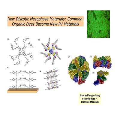
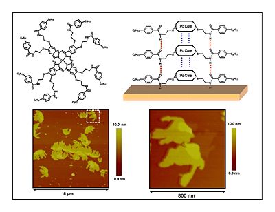
[[Image:discotic.jpg|thumb|left|400px|Another kind of thalocyanine that is solution processable form molecules that self-organize into columnar stacks. This the kind of configuration that makes molecules good light absorbers and good conductors.]] | [[Image:discotic.jpg|thumb|left|400px|Another kind of thalocyanine that is solution processable form molecules that self-organize into columnar stacks. This the kind of configuration that makes molecules good light absorbers and good conductors.]] | ||
| Line 12: | Line 96: | ||
<br clear='all'> | <br clear='all'> | ||
== Dendritic Polymers == | === Dendritic Polymers === | ||
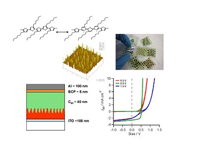
[[Image:dendriticpolymer.jpg|left|thumb|400px|Dendritic polymers create a spiky surface which may be able to be combined with an suitable electron acceptor layer to form a finely organized heterojunction.]] | [[Image:dendriticpolymer.jpg|left|thumb|400px|Dendritic polymers create a spiky surface which may be able to be combined with an suitable electron acceptor layer to form a finely organized heterojunction.]] | ||
<br clear='all'> | <br clear='all'> | ||
== Nanoparticles == | === Nanoparticles === | ||
There is research into using [[Quantum Dot Synthesis|quantum dots]] to expand OPV absorption from visible to include IR spectrum making them efficient on cloudy days. PbS is one material of interest. <ref>Colloidal PbS Nanocrystals with Size-Tunable Near-Infrared Emission: Observation of Post-Synthesis Self-Narrowing of the Particle Size Distribution" Adv. Mater. 15, 21, 1844 (2003)</ref> | |||
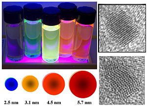
[[Image:Dyes_color.jpg|thumb|300px|Quantum dot compounds can be can be used as part of the donor or acceptor materials.]] | |||
[[Image:semicon_nanoparticle.jpg|thumb|left|400px|Semiconductor nanoparticles built from cadmium selenide 2-5nm in diameter take on interesting electron properties. The particle is capped with ligands to make them processable. The size of the nanoparticle determines the luminescence. The smallest make blue color, the largest makes the red. Used in a solar cell they absorb in the same color ranges.]] | [[Image:semicon_nanoparticle.jpg|thumb|left|400px|Semiconductor nanoparticles built from cadmium selenide 2-5nm in diameter take on interesting electron properties. The particle is capped with ligands to make them processable. The size of the nanoparticle determines the luminescence. The smallest make blue color, the largest makes the red. Used in a solar cell they absorb in the same color ranges.]] | ||
<br clear='all'> | <br clear='all'> | ||
Other research involves silver or gold nanoprisms. <ref>Metraux G.S Rapid Thermal Synthesis of Silver Nanoprisms with Chemically Tailorable Thickness Adv. Mater. 2005 17, No. 4. Feb 23</ref> <ref>C. A. Mirkin et al ,Colloidal Gold and Silver Triangular Nanoprisms small 2009, 5, No. 6, 646–664</ref> <ref>D. Aherne et al. Optical Properties and Growth Aspects of Silver Nanoprisms Produced by a Highly Reproducible and Rapid Synthesis at Room | |||
Temperature Adv. Funct. Mater. 2008,18, 2005–2016 � 2008</ref> <ref>D. J. Masiello On the linear response and scattering of an interacting molecule-metal | |||
system J. Chem. Phys. 132, 064102 �2010�</ref> | |||
See [[Wikipedia:Quantum Dots]] | |||
<br clear='all'> | |||
=== Transparent carbon nanotube electrodes === | |||
Doped carbon nanotube (CNT) electrodes can be used to create transparent electrodes which have low sheet resistance and a favorable shift of fermi level. | |||
== Tailored interfaces == | |||
<br clear='all'> | |||
== Fabrication Processes == | |||
=== Tailored interfaces === | |||
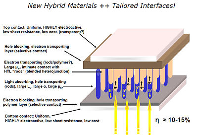
[[Image:hybrid materials.jpg|thumb|left|400px|New hybrid materials could be used to build a solar cell step by step. Light absorbing rods are placed on a transparent base. Then the electron transport rods, and the hole blocking layer.]] | [[Image:hybrid materials.jpg|thumb|left|400px|New hybrid materials could be used to build a solar cell step by step. Light absorbing rods are placed on a transparent base. Then the electron transport rods, and the hole blocking layer.]] | ||
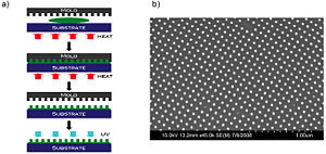
[[Image:Nanoimprinting.jpg|thumb|300px|a) Nanoimprinting process developed for organic semiconductors; b) SEM picture of nanoimprinted polycarbonate pillars 30 nm wide, 60 nm high and separated by 160 nm (center-to-center) Norwood and Peyghambarian Groups]] | |||
<br clear='all'> | |||
There are real advantages to processing methods which could easily, reproducibly and systematically nano-texture the first-deposited donor or acceptor polymer layer in an organic solar cell (OSC), forming “nano-posts” or “nano-indentations” with optimal lengths and widths, ready for addition of the second component in a bulk heterojunction (BHJ) OSC. As the aspect ratio of such a nanostructure increases, at least an order of magnitude increase in the interfacial area between the donor and acceptor phases is anticipated, thereby greatly enhancing exciton dissociation with retention of vectoral charge transport pathways. Such a processing technique, if scaled to realistic device levels, would remove one of the key limitations to BHJ formation from conventional polymeric materials. Nanoimprint lithography (NIL) involves the formation of nano-posts or nanoindentations in a reusable master stamp, which is then used to emboss a freshly deposited polymer or sol-gel oxide film. This is a process recently developed for creation of grating-like features on optical fibers and waveguides, and is now being scaled to dimensions relevant for OSC device processing. | |||
=== Solvent annealing and nanotexturing === | |||
One of the reasons that OPVs are only 5% efficient is the exciton diffusion bottleneck due to recombination of the exciton within 10nm of the interface. Unfortunately making a blended device with an ideal morphology has been difficult. | |||
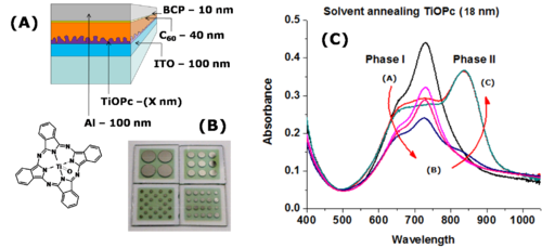
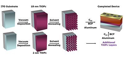
There are new strategies for producing titanyl phthalocyanine (TiOPc) and C60 heterojunctions. After deposition the material can be solvent annealed resulting in nanotexturing and tunability in the NIR. | |||
[[Image:Solvent_annealing.png|thumb|500px|TiOPc]] | |||
[[Image:Solvent_annealing_protocols.jpg|thumb|400px|]] | |||
See Armstrong <ref>N. R. Armstrong et al., Adv. Funct. Mater. ; {{Doi|10.1002/adfm.200801723}}</ref> Placencia 2009 <ref>D. Placencia, W. Wang, R.C. Shallcross, K.W. Nebesny, M. Brumbach, N.R. Armstrong, "Organic Photovoltaic Cells Based On Solvent-Annealed, Textured Titanyl Phthalocyanine/C60 Heterojunctions," Advanced Functional Materials, Vol 19, Iss 12, 1913 -1921 (2009)</ref>. | |||
See Xin 2010 <ref>Hao Xin,† Obadiah G. Reid,‡ Guoqiang Ren,† Felix Sunjoo Kim,† David S. Ginger,‡,* and | |||
Samson A. Jenekhe†,* Polymer Nanowire/Fullerene Bulk Heterojunction Solar Cells: How Nanostructure Determines Photovoltaic Properties ACS Nano, 2010, 4 (4), pp 1861–1872</ref> | |||
<br clear='all'> | |||
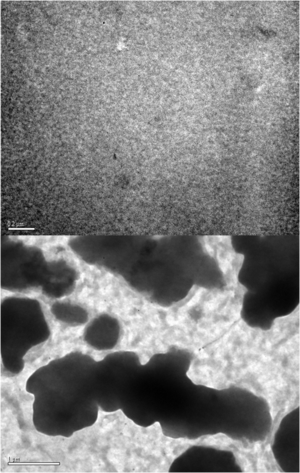
[[Image:Pcbm p3htannealing.png|thumb|300px|Transmission Electron Micrographs | |||
PCBM:P3HT 1:1 Thin film from chlorobenzene | |||
TOP: no anneal BOTTOM: 140 °C 1 h- (Black islands are N-type material]] | |||
Annealing of a blended polymer film causes a partial phase segregation into distinct islands. | |||
If a material is applied without annealing there is almost no performance because the exciton has no clear path for exciton moving. Yet the larger islands of material means a smaller interfacial area decrease the charge dissociation which again decreases the performance. | |||
<br clear='all'> | |||
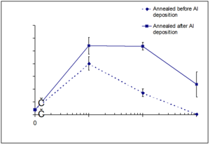
[[Image:Pcbm p3htannealing graph.png|thumb|300px|Power Conversion Efficiencies at AM 1.5 G Solar Intensity | |||
PCBM:P3HT 1:1 Thin film from chlorobenzene | |||
Annealed at 140 °C]] | |||
Luscumbe has shown that it is critical to balance these competing requirements by controlling annealing time. | |||
<br clear='all'> | |||
=== Metallic grid electrodes === | |||
One barrier to increasing the size of organic solar cells is the reduction of fill factor caused by sheet resistance of the ITO layer. | |||
Applying metal electrode grids can be employed to counter the effect of sheet resistance.<ref>Jingyu Zou, Hin-Lap Yip, Steven K. Hau, and Alex K.-Y. Jen Metal grid/conducting polymer hybrid transparent electrode for inverted polymer solar cells Appl. Phys. Lett. 96, 203301 (2010); {{Doi|10.1063/1.3394679}}</ref> | |||
== References == | |||
<references/> | |||
[[category:organic solar cell]] | |||
[[category:Materials processing and fabrication]] | |||
<table id="toc" style="width: 100%"> | |||
<tr> | |||
<td style="text-align: left; width: 33%">[[Energy vs Charge Transfer at Heterojunctions|Previous Topic]]</td> | |||
<td style="text-align: center; width: 33%">[[Main_Page#Organic Solar Cells|Return to OPV Menu]]</td> | |||
</tr> | |||
</table> | |||
Latest revision as of 16:05, 22 November 2011
| Previous Topic | Return to OPV Menu |
These are promising directions in organic photovoltaic research being pursued at the CMDITR
Evolution of Solar Cell Efficiency
These are the types of efficiencies that people have been able to reach. For example, with silicon, fill factors of about 0.8 and conversion efficiency, of 24% can be reached.
The Grätzel cell, which is a hybrid cell that has both organic and inorganic components and uses a liquid electrolyte, has a conversion efficiency of about 11%. Michael Grätzel is a professor at the technical school of Lausanne in Switzerland.
With polymers, Allen Heeger has recently reported a conversion efficiency of up to 6%. Our goal at this time is to reach the 10% efficiency in organic cells. However, it does not seem to be very easy to achieve.
| Characteristic | Silicon | Organic (Tang) | Organic (Forrest) | Organic (Graetzel) | Polymer | Hybrid nanorods |
|---|---|---|---|---|---|---|
| Open circuit voltage (Voc; V) | 0.7 | 0.45 | 1.02 | 0.721 | 0.63 | 0.7 |
| Short circuit current density (Jsc; mA/cm2) | 43 | 2.3 | 9.7 | 20.53 | 9.5 | 5.7 |
| Voc x Jsc (mW/cm2) | 30.1 | 1.035 | 9.894 | 14.80213 | 5.985 | 3.99 |
| Fill factor (FF) | 0.8 | 0.65 | 0.59 | 0.704 | 0.68 | 0.4 |
| Illumination intensity (mW/cm2) | 100 | 75 | 100 | 100 | 80 | 96.4 |
| Conversion efficiency (%) | 24.08 | 0.9 | 5.7 | 10.4 | 5.1 | 1.7 |
New materials
Research directions include using multilayers of small molecules, building polymer blends with interpenetrated networks, nanostructured oxide polymers and hybird approaches using doped inorganics in an organic matrix.
Samson Jenekhe Presentation at SPIE- Organic Photovoltaics XII Seattle Aug 22 2011
Sean Shaheen- SPIE 2010
Discotic Mesophase Materials
Dendritic Polymers
Nanoparticles
There is research into using quantum dots to expand OPV absorption from visible to include IR spectrum making them efficient on cloudy days. PbS is one material of interest. [1]
Other research involves silver or gold nanoprisms. [2] [3] [4] [5]
Transparent carbon nanotube electrodes
Doped carbon nanotube (CNT) electrodes can be used to create transparent electrodes which have low sheet resistance and a favorable shift of fermi level.
Fabrication Processes
Tailored interfaces
There are real advantages to processing methods which could easily, reproducibly and systematically nano-texture the first-deposited donor or acceptor polymer layer in an organic solar cell (OSC), forming “nano-posts” or “nano-indentations” with optimal lengths and widths, ready for addition of the second component in a bulk heterojunction (BHJ) OSC. As the aspect ratio of such a nanostructure increases, at least an order of magnitude increase in the interfacial area between the donor and acceptor phases is anticipated, thereby greatly enhancing exciton dissociation with retention of vectoral charge transport pathways. Such a processing technique, if scaled to realistic device levels, would remove one of the key limitations to BHJ formation from conventional polymeric materials. Nanoimprint lithography (NIL) involves the formation of nano-posts or nanoindentations in a reusable master stamp, which is then used to emboss a freshly deposited polymer or sol-gel oxide film. This is a process recently developed for creation of grating-like features on optical fibers and waveguides, and is now being scaled to dimensions relevant for OSC device processing.
Solvent annealing and nanotexturing
One of the reasons that OPVs are only 5% efficient is the exciton diffusion bottleneck due to recombination of the exciton within 10nm of the interface. Unfortunately making a blended device with an ideal morphology has been difficult.
There are new strategies for producing titanyl phthalocyanine (TiOPc) and C60 heterojunctions. After deposition the material can be solvent annealed resulting in nanotexturing and tunability in the NIR.
See Armstrong [6] Placencia 2009 [7]. See Xin 2010 [8]
Annealing of a blended polymer film causes a partial phase segregation into distinct islands.
If a material is applied without annealing there is almost no performance because the exciton has no clear path for exciton moving. Yet the larger islands of material means a smaller interfacial area decrease the charge dissociation which again decreases the performance.
Luscumbe has shown that it is critical to balance these competing requirements by controlling annealing time.
Metallic grid electrodes
One barrier to increasing the size of organic solar cells is the reduction of fill factor caused by sheet resistance of the ITO layer.
Applying metal electrode grids can be employed to counter the effect of sheet resistance.[9]
References
- ↑ Colloidal PbS Nanocrystals with Size-Tunable Near-Infrared Emission: Observation of Post-Synthesis Self-Narrowing of the Particle Size Distribution" Adv. Mater. 15, 21, 1844 (2003)
- ↑ Metraux G.S Rapid Thermal Synthesis of Silver Nanoprisms with Chemically Tailorable Thickness Adv. Mater. 2005 17, No. 4. Feb 23
- ↑ C. A. Mirkin et al ,Colloidal Gold and Silver Triangular Nanoprisms small 2009, 5, No. 6, 646–664
- ↑ D. Aherne et al. Optical Properties and Growth Aspects of Silver Nanoprisms Produced by a Highly Reproducible and Rapid Synthesis at Room Temperature Adv. Funct. Mater. 2008,18, 2005–2016 � 2008
- ↑ D. J. Masiello On the linear response and scattering of an interacting molecule-metal system J. Chem. Phys. 132, 064102 �2010�
- ↑ N. R. Armstrong et al., Adv. Funct. Mater. ; doi:10.1002/adfm.200801723
- ↑ D. Placencia, W. Wang, R.C. Shallcross, K.W. Nebesny, M. Brumbach, N.R. Armstrong, "Organic Photovoltaic Cells Based On Solvent-Annealed, Textured Titanyl Phthalocyanine/C60 Heterojunctions," Advanced Functional Materials, Vol 19, Iss 12, 1913 -1921 (2009)
- ↑ Hao Xin,† Obadiah G. Reid,‡ Guoqiang Ren,† Felix Sunjoo Kim,† David S. Ginger,‡,* and Samson A. Jenekhe†,* Polymer Nanowire/Fullerene Bulk Heterojunction Solar Cells: How Nanostructure Determines Photovoltaic Properties ACS Nano, 2010, 4 (4), pp 1861–1872
- ↑ Jingyu Zou, Hin-Lap Yip, Steven K. Hau, and Alex K.-Y. Jen Metal grid/conducting polymer hybrid transparent electrode for inverted polymer solar cells Appl. Phys. Lett. 96, 203301 (2010); doi:10.1063/1.3394679
| Previous Topic | Return to OPV Menu |
