Difference between revisions of "Scanning Electron Microscope"
Cmditradmin (talk | contribs) m (→Operation) |
Cmditradmin (talk | contribs) m |
||
| (23 intermediate revisions by 3 users not shown) | |||
| Line 1: | Line 1: | ||
<table id="toc" style="width: 100%"> | |||
<tr> | |||
<td style="text-align: center; width: 33%">[[Main_Page#Research Equipment, Devices and Techniques|Return to Research Tool Menu]]</td> | |||
</tr> | |||
</table> | |||
=== Overview === | === Overview === | ||
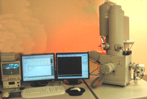
[[Image:Sirion_sem.png|thumb|300px|]] | [[Image:Sirion_sem.png|thumb|300px|]] | ||
The scanning electron microscope is used to image the surface of a conducting sample by scanning it with a high energy beam of electrons. | The scanning electron microscope is used to image the surface of a conducting sample by scanning it with a high energy beam of electrons. The SEM is a useful tool for photonics research because it reveals nano-scale surface features and topography that is critical to the performance of multi-layer devices. SEM produces dramatic pictures that reveal 3D shapes and shadows. | ||
=== Significance === | |||
Some SEMs have additional software enhancements than enable them to focus the beam on a photomask for [[E-beam lithography]] or are equipped for focused ion beam (FIB) milling. SEM can be equipped with attachments so it be used for elemental analysis using Energy Disspersive X-ray spectroscopy EDAX. | |||
=== Operation === | === Operation === | ||
Part 1 Tour and Sample Preparation | |||
{{#ev:youtube|c7EVTnVHN-s}} | |||
Part 2 Loading the Sample | |||
{{#ev:youtube|SaaVaILUObg}} | |||
Part 3 Setting the Working Distance | |||
{{#ev:youtube|CNIrvGRXugU}} | |||
Part 4 Lens Alignment and Stigmation | |||
{{#ev:youtube|NP5VckJfv04}} | |||
=== | Part 5 Moving the Stage and Imaging | ||
{{#ev:youtube|04Fvq5HWebA}} | |||
Part 6 Changing the Sample and Shutdown | |||
{{#ev:youtube|pu_pMYMYBlw}} | |||
=== Energy Dispersive X-ray Spectroscopy === | |||
Energy Dispersive X-ray Spectroscopy (EDX is used to determine the composition of a sample such as thin films. Not only can relative amounts of each atom be measured, but the distribution of the atoms in our samples can be mapped. | |||
EDX is an extension of the Sirion Scanning Electron Microscope in the Molecular Analysis Facility, make sure to watch our SEM videos before continuing. | |||
How does EDX determine composition, or, in other words, differentiate between atoms? In general, atoms are composed of nuclei (protons and neutrons) with electrons orbiting around them at different energy levels. During SEM operation, a high-energy electron beam impinges on the sample. Some of these electrons collide with electrons residing at lower energy levels, and both scatter and leave the atom. As a result, an electron located at a higher energy level sees the vacancy and jumps at the opportunity to reside at lower energy level. When the electron moves to this lower energy level, it releases energy – specifically, x-rays. Because these electron transitions are characteristic of the specific element, the energy of these x-ray emissions is also characteristic of the element. You’ll also see that multiple electron transitions for an atom are possible because electrons can fall from different elevated levels. | |||
{{#ev:youtube|pu_pMYMYBlw}} | |||
=== External Links === | |||
*[http://depts.washington.edu/cmditr/media/siriontraining_rev8_04223.pdf Training Manual for Sirion SEM] | |||
*[http://grover.mirc.gatech.edu/training/viewVideo.php?video=sem-high&size=0 Training video for Hitachi 3500H SEM at GT MiRC] | |||
*[[wikipedia:Scanning_electron_microscope Scanning Electron Microscope]] | |||
*[[wikipedia:Energy-dispersive_X-ray_spectroscopy EDAX]] | |||
[[category:Research equipment]] | |||
Latest revision as of 12:08, 17 March 2016
| Return to Research Tool Menu |
Overview
The scanning electron microscope is used to image the surface of a conducting sample by scanning it with a high energy beam of electrons. The SEM is a useful tool for photonics research because it reveals nano-scale surface features and topography that is critical to the performance of multi-layer devices. SEM produces dramatic pictures that reveal 3D shapes and shadows.
Significance
Some SEMs have additional software enhancements than enable them to focus the beam on a photomask for E-beam lithography or are equipped for focused ion beam (FIB) milling. SEM can be equipped with attachments so it be used for elemental analysis using Energy Disspersive X-ray spectroscopy EDAX.
Operation
Part 1 Tour and Sample Preparation
Part 2 Loading the Sample
Part 3 Setting the Working Distance
Part 4 Lens Alignment and Stigmation
Part 5 Moving the Stage and Imaging
Part 6 Changing the Sample and Shutdown
Energy Dispersive X-ray Spectroscopy
Energy Dispersive X-ray Spectroscopy (EDX is used to determine the composition of a sample such as thin films. Not only can relative amounts of each atom be measured, but the distribution of the atoms in our samples can be mapped.
EDX is an extension of the Sirion Scanning Electron Microscope in the Molecular Analysis Facility, make sure to watch our SEM videos before continuing.
How does EDX determine composition, or, in other words, differentiate between atoms? In general, atoms are composed of nuclei (protons and neutrons) with electrons orbiting around them at different energy levels. During SEM operation, a high-energy electron beam impinges on the sample. Some of these electrons collide with electrons residing at lower energy levels, and both scatter and leave the atom. As a result, an electron located at a higher energy level sees the vacancy and jumps at the opportunity to reside at lower energy level. When the electron moves to this lower energy level, it releases energy – specifically, x-rays. Because these electron transitions are characteristic of the specific element, the energy of these x-ray emissions is also characteristic of the element. You’ll also see that multiple electron transitions for an atom are possible because electrons can fall from different elevated levels.
