Difference between revisions of "Scanning Electron Microscope"
Jump to navigation
Jump to search
Cmditradmin (talk | contribs) m |
Cmditradmin (talk | contribs) m (→External Links) |
||
| Line 39: | Line 39: | ||
=== External Links === | === External Links === | ||
*[http://depts.washington.edu/cmditr/media/siriontraining_rev8_04223.pdf Training Manual for Sirion SEM] | |||
*[http://grover.mirc.gatech.edu/training/viewVideo.php?video=sem-high&size=0 Training video for Hitachi 3500H SEM at GT MiRC] | |||
*[[wikipedia:Scanning_electron_microscope Scanning Electron Microscope]] | |||
*[[wikipedia:Energy-dispersive_X-ray_spectroscopy EDAX]] | |||
[http://grover.mirc.gatech.edu/training/viewVideo.php?video=sem-high&size=0 Training video for Hitachi 3500H SEM at GT MiRC] | |||
[[wikipedia:Scanning_electron_microscope Scanning Electron Microscope]] | |||
[[wikipedia:Energy-dispersive_X-ray_spectroscopy EDAX]] | |||
[[category:Research equipment]] | [[category:Research equipment]] | ||
Revision as of 07:56, 3 November 2011
| Return to Research Tool Menu |
Overview
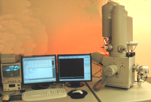
The scanning electron microscope is used to image the surface of a conducting sample by scanning it with a high energy beam of electrons. Some SEMs have additional software enhancements than enable them to focus the beam on a photomask for E-beam lithography or are equipped for focused ion beam (FIB) milling. The SEM is a useful tool for photonics research because it reveals nano-scale surface features and topography that is critical to the performance of multi-layer devices.
Significance
Operation
Part 1 Tour and Sample Preparation
Part 2 Loading the Sample
Part 3 Setting the Working Distance
Part 4 Lens Alignment and Stigmation
Part 5 Moving the Stage and Imaging
Part 6 Changing the Sample and Shutdown
