Difference between revisions of "Photonics Integration"
Cmditradmin (talk | contribs) m |
Cmditradmin (talk | contribs) |
||
| (3 intermediate revisions by the same user not shown) | |||
| Line 13: | Line 13: | ||
See Dalton 2007 <ref>http://spie.org/x16998.xml?ArticleID=x16998</ref> | See Dalton 2007 <ref>http://spie.org/x16998.xml?ArticleID=x16998</ref> | ||
See [[wikipedia:Photonic_integrated_circuit]] | |||
<br clear='all'> | <br clear='all'> | ||
| Line 29: | Line 31: | ||
[[Image:Aos_modulator.png|thumb|400px|Light can be used to change a light signal.]] | [[Image:Aos_modulator.png|thumb|400px|Light can be used to change a light signal.]] | ||
see [wikipedia: Silicon_on_insulator Silicon on Insulator] | see [[wikipedia: Silicon_on_insulator Silicon on Insulator]] | ||
[http://en.wikibooks.org/wiki/Nanotechnology/Nano-optics Wikibook on Nano optics] | |||
<br clear='all'> | |||
===References=== | ===References=== | ||
<references/> | <references/> | ||
Latest revision as of 12:03, 9 August 2010
| Previous Topic | Photonics Integration Menu |
Over the past several decades, photonics has steadily increased in importance as the preferred medium for data communications. With increased demand for higher bandwidth and more energy-efficient data transfer, optical fibers soon will replace copper wire even for simple tasks such as communications between computers and their displays as well as communications between nodes within supercomputers and microprocessors within server farms. Within such systems, optical signal processing and switching technologies have performed the relatively simple tasks of signal multiplexing, demultiplexing, amplification, routing and dispersion control. More complex tasks are typically performed electronically after optical to electrical conversion and subsequent electrical to optical conversion procedures.
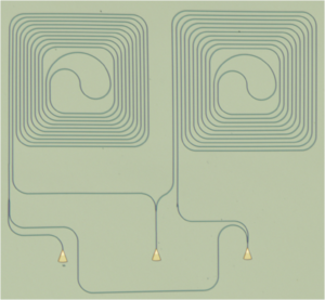
Within the past several years, lithographically defined electronic and photonic circuits have been integrated into systems that enable complex functionality. Now, it is possible to contemplate including photonic logic and storage into such circuits. In particular, such integration could lead to the opportunity of reducing the overall energy requirements of computer systems.
See Dalton 2007 [1]
See wikipedia:Photonic_integrated_circuit
Ultra low Vπ Modulators
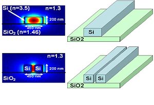
The development of waveguides with high refractive index contrast enables the confinement of light within the small mode volume of such waveguides. Miniaturization of resonators, waveguide bends, and other optical devices has resulted from creating device geometries with high refractive index contrast in easily manufacturable materials systems such as silicon on insulator (SOI).
More recently, narrow slots have been introduced into high index contrast waveguides in order to permit the introduction of gain or nonlinear material into passive devices. Surprisingly, a large fraction of the optical field can be confined within such slots in waveguides. If these slotted waveguides are constructed in a material such as silicon, which conducts and is transparent to the propagating wavelength, EO devices can be created by introducing nonlinear materials into these slots.
One remarkable property of these microfabricated Si/polymer EO modulators is that their drive current can be sub-nano-Ampere, dominated by leakage currents which are low as the polymers are excellent insulators.
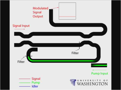
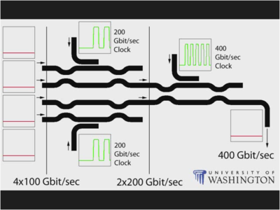
All optical on chip
see wikipedia: Silicon_on_insulator Silicon on Insulator


