Difference between revisions of "Scanning Electron Microscope"
Cmditradmin (talk | contribs) m |
Cmditradmin (talk | contribs) m |
||
| Line 1: | Line 1: | ||
<table id="toc" style="width: 100%"> | |||
<tr> | |||
<td style="text-align: center; width: 33%">[[Main_Page#Research Equipment, Devices and Techniques|Return to Research Tool Menu]]</td> | |||
</tr> | |||
</table> | |||
=== Overview === | === Overview === | ||
[[Image:Sirion_sem.png|thumb|300px|]] | [[Image:Sirion_sem.png|thumb|300px|]] | ||
Revision as of 11:21, 29 December 2009
| Return to Research Tool Menu |
Overview
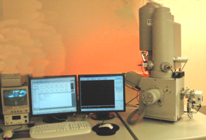
The scanning electron microscope is used to image the surface of a conducting sample by scanning it with a high energy beam of electrons. Some SEMs have additional software enhancements than enable them to focus the beam on a photomask for E-beam lithography or are equipped for focused ion beam (FIB) milling. The SEM is a useful tool for photonics research because it reveals nano-scale surface features and topography that is critical to the performance of multi-layer devices.
See Wikipedia on Scanning Electron Microscope
Operation
Part 1 Tour and Sample Preparation
Part 2 Loading the Sample
Part 3 Setting the Working Distance
Part 4 Lens Alignment and Stigmation
Part 5 Moving the Stage and Imaging
Part 6 Changing the Sample and Shutdown
Training Manual for Sirion SEM[1]
Training Video on Hitachi 3500H SEM at GT MiRC
