Difference between revisions of "Photoelectron Spectrometer XPS and UPS"
Jump to navigation
Jump to search
Cmditradmin (talk | contribs) |
Cmditradmin (talk | contribs) |
||
| Line 14: | Line 14: | ||
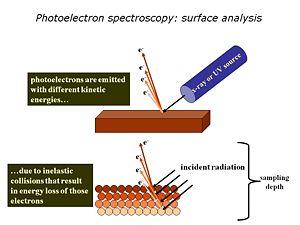
[[Image:PS-surfaceanalysis.jpg|thumb|right|300px |The small sampling depth of XPS and UPS arises because most of the photoelectrons generated do NOT make it out of the solid – they are scattered below the surface and not detected. Only those within 1-10 nm of the surface get out and can be analyzed.]] | [[Image:PS-surfaceanalysis.jpg|thumb|right|300px |The small sampling depth of XPS and UPS arises because most of the photoelectrons generated do NOT make it out of the solid – they are scattered below the surface and not detected. Only those within 1-10 nm of the surface get out and can be analyzed.]] | ||
<swf | <swf width= "640" height="480">http://depts.washington.edu/cmditr/media/pes.swf</swf> | ||
===Data interpretation=== | ===Data interpretation=== | ||
Revision as of 09:49, 22 April 2009
X-ray Photoelectron Spectroscopy and UV Photoelectron Spectroscopy are techniques for studying the surface characteristic of materials.
What is the Problem?
OLEDs and OPVs consist of thin films of organic materials, sandwiched between contacting electrodes. We need analytical tools which tell us:
- Elemental composition of metal, metal oxide and organic surfaces (top 1-10 nm)
- The molecular state of those elements in that same region
- The frontier orbital energies which control rates of charge transfer, photopotentials, onset voltages, etc.
What is our approach? Physics of XPS and UPS
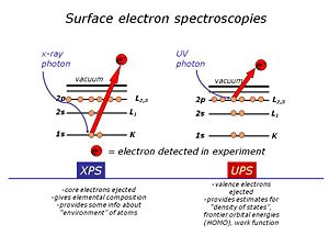
We use high-vacuum surface electron spectroscopies: X-ray photoelectron spectroscopy and UV-photoelectron spectroscopy to provide the elemental, molecular and energetic information we require about these materials.
<swf width= "640" height="480">http://depts.washington.edu/cmditr/media/pes.swf</swf>

