Difference between revisions of "Photoelectron Spectrometer XPS and UPS"
Jump to navigation
Jump to search
Cmditradmin (talk | contribs) |
Cmditradmin (talk | contribs) |
||
| Line 9: | Line 9: | ||
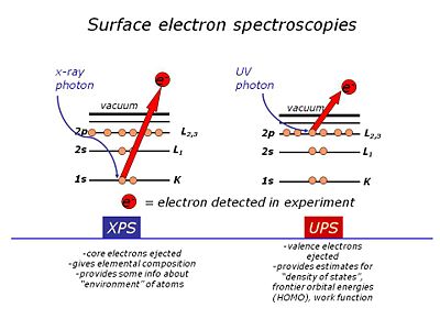
[[Image:Surface_electron_spectroscopies.jpg|thumb||400px |XPS uses high energy X-ray photons to excite “core” electrons in the near-surface region UPS uses lower energy photons in the deep UV region to excite valence electrons.]] | [[Image:Surface_electron_spectroscopies.jpg|thumb||400px |XPS uses high energy X-ray photons to excite “core” electrons in the near-surface region UPS uses lower energy photons in the deep UV region to excite valence electrons.]] | ||
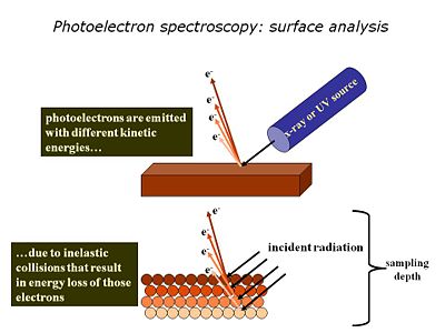
[[Image:PS-surfaceanalysis.jpg|thumb||400px |The small sampling depth of XPS and UPS arises because most of the photoelectrons generated do NOT make it out of the solid – they are scattered below the surface and not detected. Only those within 1-10 nm of the surface get out and can be analyzed.]] | |||
Revision as of 13:53, 21 April 2009
What is the Problem? OLEDs and OPVs consist of thin films of organic materials, sandwiched between contacting electrodes. We need analytical tools which tell us:
- Elemental composition of metal, metal oxide and organic surfaces (top 1-10 nm)
- The molecular state of those elements in that same region
- The frontier orbital energies which control rates of charge transfer, photopotentials, onset voltages, etc.
What is our approach? We use high-vacuum surface electron spectroscopies: X-ray photoelectron spectroscopy and UV-photoelectron spectroscopy to provide the elemental, molecular and energetic information we require about these materials.

