Conducting Tip Atomic Force Microscopy
| Return to Research Tool Menu |
Overview
Atomic Force Microscopy (AFM)is a well established process for visualizing ultrafine surface characteristics. In normal AFM scanning mode a fine needle is drawn very near a surface and is gently bent by the various atomic forces. The conducting tip gives you the chance to measure electrical conductivity at discrete locations and then correlate these measurement with the surface scan that reveals the shape.
see Wikipedia Atomic Force Microscopy
Operation
<swf width="640" height="452">http://depts.washington.edu/cmditr/media/afm.swf</swf>
Significance
This is of particular interest to the field of photonics research because the structure of thin coatings has a huge effect on the performance of devices.
Application example from Alex Veneman at U of A.:
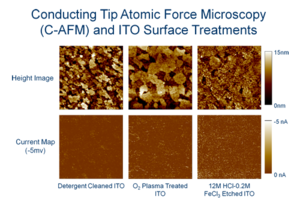
Indium Tin Oxide (ITO) is the most commonly used anode in Organic Photovoltaics (OPVs) due to its optical transparency and relatively high electrical conductivity. ITO is an imperfect electrode, and electron transfer between the ITO and adjacent organic layers is hampered by heterogeneous coverage of surface contaminants and the fact that the oxide itself is most likely a heterogeneous mixture of phases with varying electrical properties.
ITO for organic Light-Emitting Diodes (OLEDs) and OPVs is often treated by methods such as detergent or solvent cleaning, oxygen plasma or ozone cleaning and/or coating with poly(3,4-ethylenedioxythiophene) heavily doped with poly(styrenesulfonic acid) (PEDOT:PSS). The effect of these modifications at the nanoscopic level is still not fully understood, and although the effect of current-voltage properties of the devices has been studied, a working model describing their physical effects at the relevant length scales are lacking. In this work we use Conducting-Probe Atomic Force Microscopy (C-AFM) to study these surface modifications at the nanometer length scale, and compare these results to current-voltage data for macroscopic OPVs.
Our results indicate that PEDOT:PSS is a ‘band-aid’ fix for the deeper problem of heterogeneity of the ITO surface. PEDOT:PSS electrically wires over ‘dead’ spots on the ITO, making an electrically uniform electrode, but it also introduces another energy barrier to the device that increases the diode quality factor and thus decreases fill factor. We also find that aggressive acid etching of the ITO surface results in increased homogeneity, and much improved repeatability in the manufacture of devices.
