Planar Dielectric Waveguides
| Previous Topic | Return to Optical Fibers, Waveguides, and Lasers Menu | Next Topic |
Planar dielectric waveguides
Planar (slab) waveguides are the basis of waveguides used in integrated optoelectronics. The same mathematical ideas can be applied (with minor modifications) to circular waveguides.
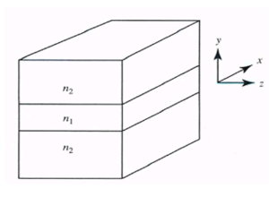
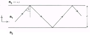
The waveguide consists of a semi-infinite slab of dielectric materials with thickness d and refractive index n1 (the core) that is sandwiched between two regions (the cladding) both of refractive index n2, and where n1>n2.
A ray of light may propagate down the core provided that total internal reflection occurs at the core/cladding interface.
this requires that:
- <math>90\deg >\theta_i > \theta_c\,\!</math>
Where
- <math>\theta_i\,\!</math> is the internal ray angle (from now on written as θ)
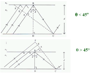
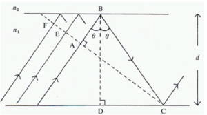
In fact there are ‘infinite” number of rays, all slightly displaced from each other, also propagating down the guide. The dotted line that is perpendicular to the wave lines is the wavefront of the propagating beam. The rays represent lines drawn normally to the plane wavefronts.
The wavefront FC intersects tow the upwardly traveling portions of the same ray at points A and C. Therefore the phase at C and A must be the same or differ by a multiple of 2π.
Otherwise there would be destructive interference between out-of-phase waves and the light will not propagate. It also requires very specific angles θ above the critical angle.
Consider the phase difference between A and C
There are two factors -the path length of AB + BC -the phase change due to reflection at B and C
We write the phase change resulting from reflection simply as δ(θ)
For perpendicular radiation φ (θ) is 2 ψ, for parallel radiation φ(θ) = 2 δ.
The total phase change is equivalent to:
- <math>(AB + BC) \frac {2\pi n_1 }{\lambda_0} - 2 \phi (\theta)\,\!</math>
Where
- <math>\lambda_0\,\!</math> is the wavelength of light in the medium
To determine the path of the light from a to b to c using trigonometry:
- <math>AB = BC cos 2 \theta\,\!</math>
Thus
- <math>AB + BC = BC(1+ cos2 \theta)\,\!</math>
Since
- <math>cos 2\theta = 2 cos^2 \theta -1\,\!</math>
- <math>AB + BC = 2 BC cos^2 \theta\,\!</math>
- <math>BD = BC cos \theta = d\,\!</math> that is the thickness of the slab
So that
- <math>AB +BC = 2d cos \theta\,\!</math>
The thickness of the slab determines the number of modes or angles that light will propagate at.
In order for the mode to propagate the total phase change must be a multiple of 2π:
- <math>\frac {4\pi n_1d cos \theta} {\lambda_0} -2 \phi (\theta) = 2m \pi\,\!</math>
- <math>\frac {2\pi n_1d cos \theta} {\lambda_0} -\phi (\theta) = m \pi\,\!</math>
Where
m is an integer
So for each value of m there will be an angle θm that satisfies the equation
Each value of θm (those >θ c) has a distinct distribution of electric field across the guide. This distribution is known as a mode. Depending on the mode there may a distribution that is centered in the core or may have 2 spots, 4 spots etc when view in cross section.
When:<math> \theta_m is = \theta_c\,\!</math> : the mode is at cut-off
If
- <math>\theta_m < \theta_c\,\!</math> : the mode is below cutoff resulting in rapid attenuation and light will not be propagated.
If
- <math>\theta_m > \theta_c\,\!</math> : the mode is above cut-off which can propagate
Mode Cut-off
The mode will be at cut-off if
- <math>\frac 2\pi n_1 cos \theta_c \lambda_0 = \pi m\,\!</math>
Since
- <math>cos \theta_c = (1-sin2\theta_c)^{1/2} = \left[ 1- \left ( n_2/n_1 \right )2 \right ]^{1/2}\,\!</math>
- <math>sin \theta_c = (n_2/n_1)\,\!</math>
Therefore mode cut-off occurs when:
- <math>\frac {2\pi d n_1} {\lambda_0} \left [ 1- (\frac {n_2}{n_1} )^2 \right ]^{1/2} = \pi m\,\!</math>
Or
- <math>V= \frac {\pi } {2} m\,\!</math>
Where
V is the normalized film thickness, normalized frequency, or V parameter
D is the thickness of the waveguide
Thus the mode shift depends on the relative index of refraction of the materials and the thickness of the waveguide. If you decrease the thickness you decrease the number of modes that can propagate.
The number of guided modes in a step-index guide (N) is given by
- <math>N= 1 + int (2V/\pi)\,\!</math>
Only one mode propagates if <math> V < \frac {\pi} {2} \,\!</math>, in this case it is called a single mode guide.
- <math>\frac {d} {\lambda_0} < \frac {1} {2(n^{2}_{1} – n^{2}_{2})^{1/2}}\,\!</math>
Example
Find the maximum waveguide core thickness d for a device with n1 =1.48 and n2 = 1.46 and a wavelength of 1 μ m to achieve single mode propagation.
- <math>d< \frac {1}{2( 1.48^2 – 1.46^2)^{1/2}} \mu m \,\!</math>
- <math>V < 2.06 \mu m\,\!</math>
| Previous Topic | Return to Optical Fibers, Waveguides, and Lasers Menu | Next Topic |


